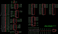
There is one register built of 74273 and 74174 that latches A5..A0, D7..D0 (both chips share the same write signal).
All bits ale cleared on power-up.

   fedcba9876543210     76543210
A~[1??.......PPw???] D~[?mPPPppp]
             ||||||     |||||+++-- PRG A16..14
             ||||||     ||+++----- PRG A19..17
             ||||||     |+-------- mirroring (0=V, 1=H)
             |||+++-----+--------- one of the bits needs to be PRG A13,
             |||                     other two need to distinguish between UNROM, NROM-32, NROM-16 and NROM-8,
             |||                     and one might be for locking writes to the regs (*)
             ||+------------------ CHR write protection (1=enabled)
             ++------------------- PRG A21..20

(*)  locking might be only used in NROM-32/NROM-16 modes; NROM-8 mode might be used only for accessing CHR data when copying them to the CHR-ROM

Because I don't know how the PAL chips works, meaning of bits A2,A0,A1,D7 is unknown

You can disable the reset signal by shorting it to +5V (short left leg of the diode with +5V)