Game Action Replay
| Type | accessory | | Mapper | | | Original mapper | | | PCB marks | NONE | | Tags: | #extra hardware | | Uploaded: | 2020-07-24 04:20:44 |
|  |
Elements:
Chip signature:
16V8+74373+74373+-(62512/621024/622048)+62256(62512/621024/622048)+GMNFC 01 OKI (QFP128)(QFP128)+7400+27512
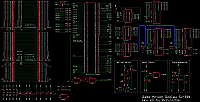
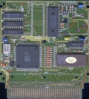
PCB top:
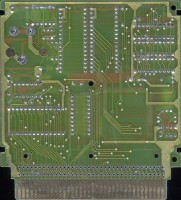
PCB bottom:
Shell top:
No photo
Shell bottom:
No photo
Screenshoots:
No photo
Extra info:
https://forums.nesdev.com/viewtopic.php?f=9&t=20529
Finally, with help of Ben Boldt, I was able to obtain QJ Game Action Replay SV-801, the famous NES add-on cartridge that can save and load game state in any moment of game. There were even no good quality photos of it in the the web, so it's high time to put it under analysis.

[size=150]The device contains:[/size]
* 16 kB 27128 EPROM,
* 32 kB 62256 SRAM (with unpopulated second slot), famous for being erased when battery runs out of its juice and bricking the cartidge,
* GMNFC 01 made by OKI, some kind of microprocessor, clocked by 20 MHz, which controls data/address/output and write enable lines of mentioned SRAM (lookind at the pins it potentially can address up to 128 kB)
* two 8bit latches, which latch address pins to the SRAM,
* GAL16V8, which switches between two RAMs
[url=https://obrazki.elektroda.pl/4125846000_1595789633_org.jpg][img]https://obrazki.elektroda.pl/4125846000_1595789633_thumb.jpg[/img][/url] [url=https://obrazki.elektroda.pl/8516243100_1595789807_org.jpg][img]https://obrazki.elektroda.pl/8516243100_1595789807_thumb.jpg[/img][/url]  [url=https://obrazki.elektroda.pl/8553926500_1595789635_org.jpg][img]https://obrazki.elektroda.pl/8553926500_1595789635_thumb.jpg[/img][/url] [url=https://obrazki.elektroda.pl/8956260600_1595789654.png][img]https://obrazki.elektroda.pl/8956260600_1595789654_thumb.jpg[/img][/url] [url=https://obrazki.elektroda.pl/3171070100_1595789680_org.jpg][img]https://obrazki.elektroda.pl/3171070100_1595789680_thumb.jpg[/img][/url] [url=https://obrazki.elektroda.pl/5045963100_1595789683_org.jpg][img]https://obrazki.elektroda.pl/5045963100_1595789683_thumb.jpg[/img][/url]

[size=150]GMNFC 01:[/size]
* This chip listens to CPU address/data bus (CPU-A14..A0, CPU-D7..D0 R/W, /ROMSEL, M2) and can drive the data bus
* It controls the CPU-A14, CPU-A13, CPU /ROMSEL, PPU-A13, PPU-/RD, CIRAM /CS, CIRAM /A10 of slave cart connector
* unrouted GMNFC 01 pins that does not seem to be connected internally: 23, 41, 56, 87, 105, 120 (other unrouted pins shows signs of internal connections during multimeter diode test)
[code]
                                                  +-------+
                                          +5V -- / 001 128 \ -- GND
                                          M2 -> / 002   127 \ -- GND
                                    CPU A11 -> / 003     126 \ <- CIR /CS
                                   CPU A12 -> / 004       125 \ <- CIR A10
                                      GND -- / 005         124 \ <- PPU /RD
                           SLAVE CPU A13 <- / 006           123 \ -> SLAVE CIR A10
                                 CPU A9 -> / 007             122 \ <- PPU A13
                         SLAVE CPU A14 <- / 008               121 \ -> SLAVE PPU A13
                               CPU A8 -> / 009                 120 \ NC
                              CPU D7 <> / 010                   119 \ -> EPR /OE
                             CPU A7 -> / 011                     118 \ -> EPR A13
                            CPU D6 <> / 012                       117 \ <- PPU A10
                           CPU A6 -> / 013                         116 \ <- CPU A13
                          CPU D5 <> / 014                           115 \ <- CPU A14
                         CPU A5 -> / 015                             114 \ ??
                        CPU D4 <> / 016                               113 \ -- +5V
                          +5V -- / 017                                 112 \ ??
                     CPU A14 -> / 018                                   111 \ ??
                        GND -- / 019                                     110 \ ??
                    CPU D3 <> / 020                                       109 \ ??
                   CPU A3 -> / 021                                         108 \ <- /RESET
                  CPU D2 <> / 022                                           107 \ <> RAM D7
                        NC / 023                                             106 \ -- +5V
                CPU A2 -> / 024                                               105 \ NC
               CPU D1 <> / 025                                                 104 \ <> RAM D5
              CPU A1 -> / 026                                                   103 \ <> RAM D6
             CPU D0 <> / 027                                                     102 \ <> RAM D4
            CPU A0 -> / 028                                                       101 \ -- XTAL
SLAVE CPU /ROMSEL <- / 029                                                         100 \ -- GND
     CPU /ROMSEL -> / 030                                                           099 \ ??
        CPU R/W -> / 031                                                             098 \ -- GND
           GND -- / 032                           GMNFC 01                            097 \ -- GND
               ?? \ 033                            OKI                                096 / ??
                ?? \ 034                                                             095 / ??
   SLAVE PPU /RD <- \ 035                                                           094 / ??
    SLAVE CIR /CS <- \ 036                                                         093 / -- +5V
                   ?? \ 037                                                       092 / ??
                    ?? \ 038                                                     091 / -- GND
                     ?? \ 039                                                   090 / ??
                      ?? \ 040                                                 089 / ??
                       NC \ 041                                               088 / ??
                        ?? \ 042                                             087 / NC
                         ?? \ 043                                           086 / -- +5V
                          ?? \ 044                                         085 / ??
                           ?? \ 045                                       084 / -- GND
                            ?? \ 046                                     083 / ??
                             ?? \ 047                                   082 / ??
                              ?? \ 048                                 081 / ??
                           +5V -- \ 049                               080 / <> RAM D2
                                ?? \ 050                             079 / ??
                                 ?? \ 051                           078 / <> RAM D3
                                  ?? \ 052                         077 / -- GND
                                   ?? \ 053                       076 / <> RAM D0
                                    ?? \ 054                     075 / <> RAM D1
                                     ?? \ 055                   074 / -> LA04 / LA00
                                      NC \ 056                 073 / -> LA07 / LA12
                                       ?? \ 057               072 / -> LA03 / LA06
                                   ALE1 <- \ 058             071 / -> LA10 / LA08
                                 RAM /WE <- \ 059           070 / -> LA14
                                          ?? \ 060         069 / -> LA16 / LA13
                                      ALE2 <- \ 061       068 / -> LA15 / LA09
                                    RAM /OE <- \ 062     067 / -> LA05 / LA02
                                         GND -- \ 063   066 / -> LA01 / LA11
                                          GND -- \ 064 065 / -- +5V
                                                  +------+/
[/code]

[size=150]GAL:[/size]
* equations derived basing on its operation:
[code]
  RAM1_nCS <= (ALE2) | (RAM_A15);
  RAM2_nCS <= (!RAM_A15) | (ALE2);
  RAM1_nWE <= (RAM_A15) | (RAM_nWE);
  RAM2_nWE <= (!RAM_A15) | (RAM_nWE);
  RAM_A14  <= LA14 when ALE2 = '1'         ;latch

  CLKOUT (pin 19) - sems too be unused input
  CLKIN (pin 1) - seems to be unused input
[/code]
* I was able hovewer to read-it back in TLS866 programmer and then program different GAL using this jedec file and it seems to behave the same, so looks like it was not protected - I attach the GAL jedec fusemap:


[size=150]Memory map (after powerup):[/size]
$5000-$5fff -> RAM (*)
$8000-$bfff -> open bus
$c000-$ffff -> EPROM
(*) The content of memory was corrupted, but I found a file named GAR.BIN in CopyNES' plugins directory which is believed to be the file used to reprogram the SRAM and fix the cartridge)

[size=150]Principle of operation[/size]
I replaced the battery and wanted to fix the SRAM content by reprogramming it using MyKazzo (I don't have CopyNES), but reading $5000-$57ff region returns inconsistent results. I will examine how the GMNFC 01 chip works, but at this moments I can say it behaves weird - it does not behave like ASIC chip, but rather like a microcontroller that executes its code cycle by cycle.
For example, at the start of CPU read $5200 cycle I expected that it would quickly latch address to the RAM (ALE1, ALE2), then enable it (RAM /OE), then read its content (RAM D7..D0) and pass the data to the CPU bus (CPU D7..D0), but it looks like when M2 is high, RAM /OE is asserted twice and ALE1/ALE2 also togggls multiple times
[url=https://obrazki.elektroda.pl/6359446900_1595790337.png][img]https://obrazki.elektroda.pl/6359446900_1595790337_thumb.jpg[/img][/url]

I extendend the M2 much longer and RAM /OE, ALE1 and ALE2 toggled more times. Looks like the M2 period must match the one in real hardware. When M2 is low, RAM /OE is high but ALE1 and ALE2 are still toggling.

One of few photos in the internet shows that the menu should looks like:
[img]https://obrazki.elektroda.pl/5508542600_1595789844.jpg[/img]

On power up, the EPROM code makes some writes:
$4182 <- 00
$418B <- 00
$418D <- 00
$4185 <- A7
and then jumps to $5200


To be continued...
Comments:
Want to leave a comment?