Shell bottom: No photoScreenshoots: No photoExtra info:
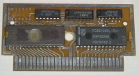
This one is internesting. The equivalents of russian chips are:
KR1533LL1 = SN74ALS32
K555IE10 = 74LS161
K555LA3 = SN74LS00

But I don't see here enough logic to support this:
[code]
$8001, mask: f0001:
[.... ...m]
         +-- mirroring (0=V, 1=H)

$9001, mask: $f001:
[.... PPP.]
      +++--- 16kB PRG bank at $8000

$8000 | $ffff
------+-------
 PPP  |   7
[/code]

Maybe $8000 and $9001 are merged into one register (that would make sense because they use different data line.
* 4/4 of 7400 might be used for mirroring mux
* 3/4 of 7432 for OR-ing A14 with PRG-A14/15/16 for last bank.
* 1/4 of 7432 for ORing /ROMSEL and CPU-A14 to make the reg appear at $8000-$BFFF (?)

Note the unpopulated place for DIL14 chip.


Do you have back-side photo of this PCB?