Harvest Moon
Elements:
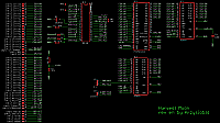
Chip signature:
6264A+6264A+DIL40+MX29L1611(27C320)
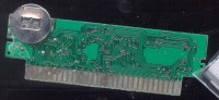
PCB top:
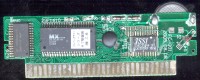
PCB bottom:
Shell top:

Shell bottom:
No photo
Screenshoots:

Extra info:
http://forums.nesdev.com/viewtopic.php?f=3&t=18000

I've analyzed the PCB with `Mu Chang Wu Yu (Harvest Moon) (NJ011) (Redump) (Unl) (Ch)` game (which has mapper 163 assigned). Only D7/D3..D0s are routed to the mapper, so not all features described by you are even persent, but here are more details about $5300 (game dump with $5300=3 matches the one from database).
I was analyzing another cartridge with mapper 163 today (Diablo 2) and also when $5300=0, two inner bank bits seems to be ored with 3.

[url=https://obrazki.elektroda.pl/6803825700_1583712578.png][img]https://obrazki.elektroda.pl/6803825700_1583712578_thumb.jpg[/img][/url]
[url=https://obrazki.elektroda.pl/7447303400_1583712584_org.jpg][img]https://obrazki.elektroda.pl/7447303400_1583712584_thumb.jpg[/img][/url] [url=https://obrazki.elektroda.pl/6156301800_1583712587_org.jpg][img]https://obrazki.elektroda.pl/6156301800_1583712587_thumb.jpg[/img][/url]

[code]
PCB: FC-001 2005.08.08
Game: Mu Chang Wu Yu (Harvest Moon) (NJ011) (Redump) (Unl) (Ch) [!].nes

Mapper pinout (this is epoxy blob):
                     .----v----.
   (n/c)       NC -- | 01   34 | -- +3.3V
         WRAM /CE <- | 02   33 | -> PRG A20 ($5200.1)
PRG A19 ($5200.0) <- | 03   32 | -> n/c     ($5200.2)
    n/c ($5100.0) <- | 04   31 | <- n/c     ($5100.2) internally pulled down
PRG A18 ($5000.3) <- | 05   30 | <- CPU D0
          PPU A13 -> | 06   29 | <- CPU D1
          PPU A9  -> | 07   28 | <> CPU D2
          PPU /RD -> | 08   27 | <- CPU D3
          PPU A12 -> | 09   26 | <- CPU D7
          CHR A12 <- | 10   25 | -- GND
          VBAT    -- | 11   24 | <- CPU M2
          RAM VCC -- | 12   23 | <- CPU /ROMSEL
        +5V--100R -- | 13   22 | <- CPU A14
PRG A17 ($5000.2) <- | 14   21 | <- CPU A13
PRG A16 ($5000.1) <- | 15   20 | <- CPU A12
PRG A15 ($5000.0) <- | 16   19 | <- CPU A10 or CPU R/W
          CPU A8  -> | 17   18 | <- CPU A9
                     '---------'

* Voltage applied to the WRAM via pin 12 = OR(pin 11, pin 13)

* Because of the following wiring:
      CPU R/W --->|---+
      CPU A10 --->|---+-- pin 19 of mapper epoxy
      GND     --[1k]--+
- all writable ports must have A10=0 (mask: $F700)
- all readable can have any A10 (mask $F300)

* All bits in registers seem to be 0 on powerup

* Write registers:
  /RM CPU CPU CPU CPU CPU
  SEL A14 A13 A12 A09 A08
   1   1   0   0   0   0  $4000 [........]
   1   1   0   0   0   1  $4100 [........]
   1   1   0   0   1   0  $4200 [........]
   1   1   0   0   1   1  $4300 [........]

   1   1   0   1   0   0  $5000 [V...abcd]
                                 |   ||||
                                 |   ++++- PRG-A18,A17,A16,A15
                                 +-------- 0: CHR A12 always follows PPU A12
                                           1: During rising edge of PPU A13, PPU A9 is latched.
                                              No matter if that was read or write. Then this A9
                                              is used as CHR A12 but only for reads (only when PPU /RD=0)
                                              (for writes - CHR A12 always follows PPU A12)

   1   1   0   1   0   1  $5100 [......BA]
                                       |+- bit output on pin 4 (when $5300.0 = 0)
                                       +-- bit output on pin 4 (when $5300.0 = 1)

   1   1   0   1   1   0  $5200 [.....PPP]
                                      +++- PRG-A21,A20,A19

   1   1   0   1   1   1  $5300 [.....D.F]
                                      | |
                                      | +---- Swap two lowest bits for further writes to $5000/$5100/$5200 (0=no, 1=yes)
                                      +------ What to drive PRG-A18..15 with (0=ab11, 1=abcd)

Notes:
* "swap two lowest bits" means that writing to $5300 does not change the current value of $5000/$5100/$5200.
  Only next write to $5000/$5100/$5200 will make effect.
* "use ab11" means that writing to $5300 immediatelly changes what is wired to PRG-A18..15
  Example1:
  $5300 <- 00000000
  $5200 <- 00000001
  $5000 <- 00000001
  ;$8000  points to bank 19
  $5300 <- 00000100
  ;$8000  points to bank 17
  $5300 <- 00000101
  ;$8000  points to bank 17
  $5000 <- 00000001
  ;$8000  points to bank 18
  $5200 <- 00000001
  ;$8000  points to bank 34

  Example2:
  $5300 <- 00000000
  $5100 <- 00000001
  ;pin 4 is HIGH
  $5300 <- 00000001
  ;pin 4 is HIGH
  $5100 <- 00000001
  ;pin 4 is LOW
  $5300 <- 00000000
  ;pin 4 is LOW

* Read registers:
  /RM CPU CPU CPU CPU CPU
  SEL A14 A13 A12 A09 A08
   1   1   0   0   0   0  $4000 [........]
   1   1   0   0   0   1  $4100 [........]
   1   1   0   0   1   0  $4200 [........]
   1   1   0   0   1   1  $4300 [........]
   1   1   0   1   0   0  $5000 [........]
   1   1   0   1   0   1  $5100 [.....Z..]
                                      +--- bit read from pin 31
   1   1   0   1   1   0  $5200 [........]
   1   1   0   1   1   1  $5300 [........]
[/code]

--

[quote]
Many thanks. All of my analysis comes from debugging the games, so insight from actual PCBs is always appreciated.
[/quote]
Unbelievable, I was thinking your description are based on hardware testing. You are genius then.

I made few mistakes, here are erratas (I already fixed them in above description):
1. `Mu Chang Wu Yu (Harvest Moon) (NJ011) (Redump) (Unl) (Ch)` is assigned into mapper 163, not 164 (the correct one)

2. The layout of the ROM matches the dump with $5300=4, not the $5300=7  (when $5300=4, the order of signals going to A20..A15 is non swapped )

4. The last line of example should be `  ;$8000  points to bank 34`, not  ` ;$8000  points to bank 28`

[quote]
"Nong Chang Xiao Jing Ling 农场小精灵" (NJ025), which is Nanjing's re-release of Harvest Moon with a new title screen, depends on PRG A15 coming from $5100 D1 when (and only when) $5300=$04. Could you please check again if this is the case on the PCB you studied, or whether $5100 D1 instead of D0 can be output on any pin when $5300=$04?
[/quote]
Yup, looks like $5300.0 also swaps two lowest $5100 bits (see updated description and example 2).
Also I tested and when reading, $5100.2 is always connected to pin 31, despite of $5300.

-

I started my work on mapper 163 because one of the guys noticed me that "Diablo (NJ037) (Unl) (Ch) [!]" [mapper 163] glithes (screen blinks) on the final screen (where automatic CHR switching is used), but title screen which uses the same technique works. This behaviour appears in FCEUX as well as in my hardware reproduction cartridge (which is technically based on FCEUX).
[img]https://obrazki.elektroda.pl/7661070800_1583761699.png[/img].
He has the original cartridge and it does not suffer from that bug:
[url=https://obrazki.elektroda.pl/1294232300_1583761770.jpg][img]https://obrazki.elektroda.pl/1294232300_1583761770_thumb.jpg[/img][/url]

It turned out that his cartridge is in fact `Diablo (NJ037) - Anhei Pohuai Shen - Diablo - Repro (Unl) (Ch) [!]` (which differs in few places, for example - it writes to $5300 value 7, while the first one writes 4), but after dumping and playing on emu - it still suffers from the same bug. BTW. The dump of this `Diablo (NJ037) - Anhei Pohuai Shen - Diablo - Repro (Unl) (Ch) [!]` with $5300=7 matches the one from database.
I am wondering if it is because the title screen is static, and the final screen has text constantly being updated (and when writing, CHR A12 always follows PPU A12).

Anyway, he was so kind and make photos of his PCB. After a long guessing I think I got the schematic. the mapper epoxy (top) seems to have identical pinout as from the Harvest Moon! There is second small blob (bottom) that wires (probably):
PRG-A21, PRG-A20, PRG-A19, PRG-A18, PRG-A17, CPU-R/!W, $5100.0, M2, D2. I wonder if this isnt some serial eprom memory? That would agree with you research that bits from the $5200 (which are used as high bits) are reused for EPROM!
There are also a some unused pads in top-left region (for jumpers), one of them is RD_$5100.2. By making physical connections they could achieve different things to be connectedto $5100.2.

[url=https://obrazki.elektroda.pl/4277632800_1583765791_org.jpg][img]https://obrazki.elektroda.pl/4277632800_1583765791_thumb.jpg[/img][/url] [url=https://obrazki.elektroda.pl/8702374400_1583765796_org.jpg][img]https://obrazki.elektroda.pl/8702374400_1583765796_thumb.jpg[/img][/url] [url=https://obrazki.elektroda.pl/9099029600_1583765795.png][img]https://obrazki.elektroda.pl/9099029600_1583765795_thumb.jpg[/img][/url]


--


Sorry for the delay but while trying to change it into flashable cartridge, I encoutered a lot of weird problems.
1) First one - before even modyfing the cartridge I found out that the graphics on bottom half of screen (due to the automatic VRAm-A12 switch) is incorrect on some nes-on-chip consoles (just like the switching wouldnt happen), and on chipped ones - there are random artifacts.
-Adding 220pf between PPU-A13 and GND solved problems on NOC, but not on chipped console.
-Adding 47uf on +5.5V and +3.3V solved problems, but then the cartridge didn't wanted to boot on first time (oddly, after pressing reset it starts - wtf?)
[img]https://obrazki.elektroda.pl/4577726100_1583881478.gif[/img]

2) Then I disconnected /WE from the flash and connected to CPU R/W and disconnected /OE and connected to negated CPU R/W. After a few resets I found out that the cartridge stopped working. Reading back memory shown that some cells changed their value (spurious writes? - wtf2)

2) Then I studied datasheet of this 29L1611MC memory to implement the write operations in Kazzo. It is different from the regular flashes (example - 29F040, 39SF040).
* First, because all fifteen address bits are important during decoding commands, but that's not problem because due to 32k bank, all bits can be controlled.
* Second, because even in 8-bit mode (when /BYTE pin is pulled low), memory watches for its A14..A0, not A13..A-1 when decoding commands (this is different for example in comparision to 29L320) This means that outputing those 5555/2AAA commands involves PRG-A15, CPU-A14...CPU-A1, so every write command need writing to mapper register - going to be veeeeery slow?
* Third because there is no automatic polling, but instead - I need to issue `read status register` command and after it - I need to issue `go back to read mode` command
* Fourth, memory has  page mode, which allows writing up to 128 bytes at once (and I need to use it, because writing byte per byte would be extremely slow)

3) I spend few hours trying to figure out why still I can't read exactly what I programmed into chip. For example, writing at locations $D300-$D3FF caused some weird behaviour. Then I found out that this location corresponds to $5300-$53FF. If /ROMSEL goes low too late (like in Kazzo), mapper thinks that we wanted to write to $5300-$53ff and switches bank in the midle of write cycle. As a result, memory chip behaves even more weird, because it goes and stays in status read mode (!)
I thought this mapper blob latches data on falling edge of M2, where /ROMSEL is correct. So either it does not totally respect /ROMSEL while writing, or  there must be some kind of delay circuitry inside.
[url=https://obrazki.elektroda.pl/5033581800_1583877864.png][img]https://obrazki.elektroda.pl/5033581800_1583877864_thumb.jpg[/img][/url]

Anyway, the cartridge is ready:
[url=https://obrazki.elektroda.pl/3275202800_1583881382_org.jpg][img]https://obrazki.elektroda.pl/3275202800_1583881382_thumb.jpg[/img][/url] [url=https://obrazki.elektroda.pl/5971393200_1583881384_org.jpg][img]https://obrazki.elektroda.pl/5971393200_1583881384_thumb.jpg[/img][/url]

--

I programmed Wacraft to it and all I got was this checkboard screen (with title music playing in the background). After pressing start, game hangs. Exact the same behaviour that if I played the ROM in emulator basing on my implementation of this mappe.
[img]https://obrazki.elektroda.pl/4078626800_1583881583.png[/img] (WHen I programmed back the Harvest Moon, of course it works normally)

I am going to trace your photos to see what is the difference.

BTW. Good game for testring the 'read-only' behaviour of auto chr switch is "San Guo Wu Shuang - Meng Jiang Zhuan (C)", because it does it just on title screen, no need to play till the end of Diablo.
Comments:
Want to leave a comment?