Can you help getting more info about those carts?
| Unique visits: 7790 Can you help getting more info about those carts? |
|  |
| Name | Value |
|---|---|
| IC1 | 27C320 |
| IC2 | 27F080 |
| IC3 | DIL64 |
| C1 | - |
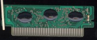
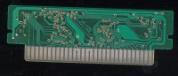
| CART1 | FAMICOM_CART |
| JP1 | 2-3 |
| JP2 | open |
| JP3 | 1-2 |
| JP4 | cut trace |
| R1 | 2.2k (not soldered) |
| R2 | 470 |
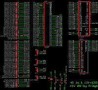
JY-120 (45 in 1) - reverse engineering results.

PCB: 2 MB PRG-ROM (blob) + Mapper BLOB (55 pins) + 1 MB CHR-ROM (blob)

Mapper BLOB pinout (pin 1 is the first pin after VCC with counter-clockwise counting)
                +-----------+
M2           -> | 1      10 | -> PRG-!CE
CPU-!ROMSEL  -> | 3      53 | -> PRG-A20
CPU-R/!W     -> | 42     52 | -> PRG-A19
CPU-A14      -> | 6      51 | -> PRG-A18
CPU-A13      -> | 5      50 | -> PRG-A17
CPU-A12      -> | 4      49 | -> PRG-A16
CPU-A11  (*) -> | 54     48 | -> PRG-A15
CPU-A2       -> | 9      47 | -> PRG-A14
CPU-A1       -> | 8      46 | -> PRG-A13
CPU-A0       -> | 7         |
                |           |
PPU-!RD      -> | 41      2 | -> CHR-!CE
PPU-A13      -> | 22     23 | -> CHR-A19 (***)
PPU-A12      -> | 21     43 | -> CHR-A18
PPU-A11      -> | 20     40 | -> CHR-A17
PPU-A10      -> | 19     39 | -> CHR-A16
PPU-A9       -> | 31     38 | -> CHR-A15
PPU-A8       -> | 30     37 | -> CHR-A14
PPU-A7       -> | 29     36 | -> CHR-A13
PPU-A6       -> | 28     35 | -> CHR-A12
PPU-A5       -> | 26     34 | -> CHR-A11
PPU-A4       -> | 25     33 | -> CHR-A10
PPU-A3       -> | 24        |
                |           |
CPU-D0      <-> | 11        |
CPU-D1      <-> | 12        |
CPU-D2      <-> | 13        |
CPU-D3      <-> | 14        |
CPU-D4      <-> | 15     44 | -> CIRAM-A10
CPU-D5      <-> | 16        |
CPU-D6      <-> | 17     45 | -> !IRQ
CPU-D7      <-> | 18        |
                |        55 | - VCC
DIPSW (**)   -> | 32     27 | - GND
                +-----------+

				Notes:
(*) There is a solder jumper selecting between connecting this to CPU-A11 and GND
(**) There is a solder jumper selecting between GND and VCC (tied to GND)
(***) There is jumper allowing to connect this pin to either GND/VCC/open

Interesting is fact for routing PPU-A9..3, but the described mapper behaviour does not utilize them.

Unfortunatelly my PCB has some of the lines broken (they were sitting at around 0.5V):

* prg-a14, prg-a15, prg-a16
* prg-a13, prg-a19
* prg-a15
* chr-a11, chr-a19
* chr-!ce

[10.. ....] $5000-$57ff: DIP switch setting (read)
 | || ||||
 | ++-++++- open  bus
 +--------- value of pin 32 (DIPSW solder jumper)

[C....PPC] D003
 |    |||
      |++- outer CHR(A19,A18)
	  ++-- outer PRG(A20,A19)


$9000-$9007 regs : [CCCCCCCC]
$9000-$9000: [CCCCCCCC]


---

For example, If I write:
$5800 <- $00
$5801 <- $00
to clear internal values), wait 8 M2 cycles and then write:
$5800 <- $ff
$5801 <- $08
Then successive reads of $5800 will return:
00 00 00 80 c0 e0 f0 f8
If I then repeat the whole procedure from start then successive reads of $4801 will return:
00 00 00 7f 3f 1f 0f 07

reg : std_logic_vector(15 downto 0);
if reg5800_write = '1' then
	reg5800 <= cpu_data;
elsif reg5801_write = '1' then
	reg5801 <= cpu_data;
	mult_cycle <= 0;
elsif rising_edge(cpu_m2) and mult_cycle < 8 then

        11111111
	  * 00001000
----------------
        00000000
       00000000
      00000000
     11111111

0000000000000000
0000000000000000
0000000000000000
0111111110000000
0011111111000000
0001111111100000
0000111111110000
0000011111111000
Comments: