15 in 1
| Type | multi | | Mapper | 916 | | Original mapper | 0+2 | | PCB marks | 891227 | | Tags: | | | Uploaded: | 2019-08-12 10:30:46 |
|  |
Elements:
Chip signature:
27F080+27512+6264+74138+74153+74174+74174+16L8
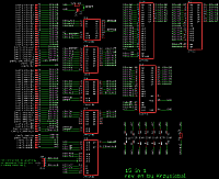
PCB top:
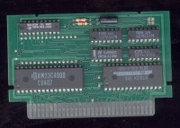
PCB bottom:

Shell top:
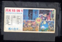
Shell bottom:

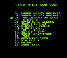
Screenshoots:
Extra info:
15 in 1 multicart (NROM/UNROM + $6000)

Funny NROM/UNROM multicart that also maps ROM at $6000 (in fact, the whole menu code is ran only from $6000-$7fff)
Whats the point of writing game sizes on the label? And look at the back of the shell :D

[url=https://obrazki.elektroda.pl/8172742400_1570306436.jpg][img]https://obrazki.elektroda.pl/8172742400_1570306436_thumb.jpg[/img][/url]

[code]
PRG:
  ROM1 512 kB,
  ROM2 128kB, unpopulated
CHR:
  RAM 8 kB, can be write protected

Bus conflicts: no

REGISTERS (both cleared on powerup but NOT reset):
  $8000-bfff:
     fedcba9876543210     76543210
  A~[10w.............] D~[ABCDE...]
       |                  |||||
       |                  |||++---- PRG outer bank
       |                  |++------ PRG mode: 00=NROM 16k, 01=NROM 32k, 10/11=UNROM,
       |                  |++------ PRG chip select: 00/01/10=PRG1, 11=PRG2
       |                  |+------- CHR-ROM write protection: 0=enabled, 1=disabled
       |                  ++------- mirroring: 00=V, 10=H, 01/11=1ScB(CIR_A10=VCC)
       +--------------------------- write protection of both registers: 0=disabled, 1=enabled

  $c000-ffff:
     fedcba9876543210     76543210
  A~[11..............] D~[.....FGH]
                               |||
                               +++- PRG inner bank (H ignored in NROM 32k)

$6000 mapped to second half of first 16kB from PRG1 (second 8kB bank)

BC | $6000       | $8000      | $c000
00 | PRG1=000001 | PRG1=DEFGH | PRG1=DEFGH
01 | PRG1=000001 | PRG1=DEFG0 | PRG1=DEFG1
10 | PRG1=000001 | PRG1=DEFGH | PRG1=DE111
11 | PRG1=000001 | PRG2=DEFGH | PRG2=DE111


PAL equations:
  PRG2_nCE = (!CPU_RnW) | (!REG1_D5) | (!REG1_D6) | (CPU_nROMSEL);
  PRG1_nCE = (REG1_D6 & REG1_D5 & !CPU_nROMSEL) | (!CPU_A14 & CPU_nROMSEL) | (!CPU_A13 & CPU_nROMSEL) | (!CPU_RnW);
  PRG_A18 = (REG1_D4 & !CPU_nROMSEL);
  PRG_A17 = (REG1_D3 & !CPU_nROMSEL);
  PRG_A16 = (REG1_D6 & CPU_A14 & !CPU_nROMSEL) | (REG2_D2 & !CPU_nROMSEL);
  PRG_A15 = (REG1_D6 & CPU_A14 & !CPU_nROMSEL) | (REG2_D1 & !CPU_nROMSEL);

  PRG_A14 = (!REG1_D5 & REG2_D0 & !CPU_nROMSEL) |
            (REG1_D5 & CPU_A14 & !CPU_nROMSEL) |
            (REG1_D6 & REG2_D0 & !CPU_nROMSEL) |
            (REG1_D6 & CPU_A14 & !CPU_nROMSEL);

[/code]

[url=https://obrazki.elektroda.pl/5319640000_1570306059.jpg][img]https://obrazki.elektroda.pl/5319640000_1570306059_thumb.jpg[/img][/url] [url=https://obrazki.elektroda.pl/8222997800_1570306062.jpg][img]https://obrazki.elektroda.pl/8222997800_1570306062_thumb.jpg[/img][/url] [url=https://obrazki.elektroda.pl/3334790600_1570306065.jpg][img]https://obrazki.elektroda.pl/3334790600_1570306065_thumb.jpg[/img][/url] [url=https://obrazki.elektroda.pl/5958301600_1570306067.jpg][img]https://obrazki.elektroda.pl/5958301600_1570306067_thumb.jpg[/img][/url] [url=https://obrazki.elektroda.pl/2641453400_1570306094.png][img]https://obrazki.elektroda.pl/2641453400_1570306094_thumb.jpg[/img][/url] [url=https://obrazki.elektroda.pl/6250049400_1570306097.png][img]https://obrazki.elektroda.pl/6250049400_1570306097_thumb.jpg[/img][/url]

--

There is a jumper in the PCB, used to select what goes to CIRAM-A10 when 01/11 is writen to mirroring register bits:
* open (like on my PCB) -> single screen mirroring.
* closed 1-2 -> V
* closed 3-4 -> H

[url=https://obrazki.elektroda.pl/2846694000_1570309670.png][img]https://obrazki.elektroda.pl/2846694000_1570309670_thumb.jpg[/img][/url] [url=https://obrazki.elektroda.pl/4386206500_1570310005.png][img]https://obrazki.elektroda.pl/4386206500_1570310005_thumb.jpg[/img][/url]
Comments:
Want to leave a comment?