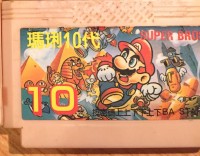
Super Mario 10 (chips)
| Type | single | | Mapper | | | Original mapper | 4 | | PCB marks | 92 719 | | Tags: | | | Uploaded: | 2022-11-26 10:11:51 |
|  |
Elements:
Chip signature:
2C(27512)+7402 (not soldered)(7402)+AX5202P(MMC3)+2732(27512)+2D(27512)+27c512(27512)+7400+74138+7432+7400+74138
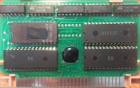
PCB top:
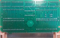
PCB bottom:
Shell top:
Shell bottom:
No photo
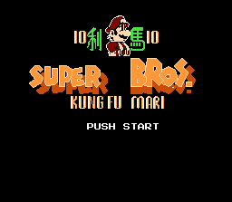
Screenshoots:
Extra info:
http://forums.nesdev.com/viewtopic.php?f=9&t=19284
While checking the original releases of the infamous Super Bros. hacks, I remembered that my two copies of the Jackie Chan one (Super Bros. 10) had different PCBs. The small one revealed to be M196, like most of those hacks. However the large one, which at first was a candidate for an original print with an obscure mapper, showed to be just standard MMC3.
Was this meant to be a 2-in-1 MMC3 multicart with two 2x128kB games? Clues on the reason for the 4kB UVEPROM?
--
I compared [i]Super Bros 10 Kung Fu Mari.nes[/i] against [i]USA\Jackie Chan's Action Kung Fu (U).nes[/i] and they seems to be almost same, differences, here are difference regions:
PRG:
D65B-D698 copyright information cut off
F85F-F861 ?
FB06-FB08 ?
FB0E ?
FDF9 ?
1C284, 1C292, 1C737 (*)
1CA8D ?
1CA91 ?
1CAE8 ?
1CF1E ?
1CF23 ?
1DD18, 1E1AB, 1E1B1, 1E1DF, 1E20F, 1E215, 1E29B, 1E2D0, 1E3AC, 1F53B, 1F548, 1F6E8, 1F83A, 1FD72 (*)
(*) = those refers to the fact that Jackie Chans Use 8001/E001/C001 while Super Bros 10 - 8005/E005/C005 (which is irrelevant cause for MMC3 is the same)
CHR:
2E111-38B9A (less than 64k)
No idea why the patch and whole logic instead of just putting EPROMs with altered PRG/CHR.
-
Ok I think I got it.
PRG:
Assuming they wanted to patch the above regions marked as (?), they needed to cover those 2 regions:
[code]
$0f800-$0ffff = 011111xxxxxxxxxxx
$1c800-$1cfff = 111001xxxxxxxxxxx
||||||
|||||+- CPU A11
||||+-- CPU A12
|||+--- MMC3 PRG A13
||+---- MMC3 PRG A14
|+----- MMC3 PRG A15
+------ MMC3 PRG A16
[/code]
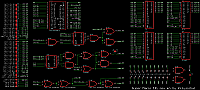
Which is perfectly done using the following circuit:
[url=https://obrazki.elektroda.pl/8796861500_1568569390.png][img]https://obrazki.elektroda.pl/8796861500_1568569390_thumb.jpg[/img][/url]
Connecting 2732.A11 to MMC.A16 causes the first 2 kB of 2732 EPROM to store the first region and the second 2kB the other.
-
CHR:
By dividing the whole CHR into eight 16k regions and counting how many bytes in that regions differ shows that there are only four regions that need to be patched.
[code]
region # diffs
$00000-$03fff: 0 000
$04000-$07fff: 0 001
$08000-$0bfff: 0 010
$0c000-$0ffff: 2747 011 - fourth 16k in 27c512
$10000-$13fff: 4660 100 - first 16k in 27c512
$14000-$17fff: 3248 101 - second 16k in 27c512
$18000-$1bfff: 1118 110 - third 16k in 27c512
$1c000-$1ffff: 0 111
|||
||+- MMC3 CHR A14
|+-- MMC3 CHR A15
+--- MMC3 CHR A16
[/code]
Which is perfectly done using the following circuit:
[url=https://obrazki.elektroda.pl/9699961000_1568569479.png][img]https://obrazki.elektroda.pl/9699961000_1568569479_thumb.jpg[/img][/url]
The missing 7402, if soldered (without 74138/7432/7400) makes the PCB usable as regular MMC3 with two 64K standard CHR-EPROMS. There must be some jumpers underneath CHR-ROM however that disconnects MMC3-CHR-A16 from its pin1.
There is no way to read-back unmodified parts of 2C and 2D mask roms without cutting some traces or desoldering them.
[url=https://obrazki.elektroda.pl/2548495200_1568569616.png][img]https://obrazki.elektroda.pl/2548495200_1568569616_thumb.jpg[/img][/url] [url=https://obrazki.elektroda.pl/4597477800_1568569624.png][img]https://obrazki.elektroda.pl/4597477800_1568569624_thumb.jpg[/img][/url] Comments:
Want to leave a comment?