Dahua Sanguo (Yancheng YC-03-09 PCB)
Elements:
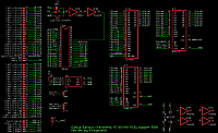
Chip signature:
6264+?(93C46)+27F080+6264+DIL40+7404
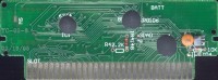
PCB top:
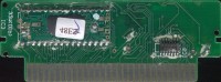
PCB bottom:
Shell top:
No photo
Shell bottom:
No photo
Screenshoots:
No photo
Extra info:
Dahua Sanguo (Yancheng YC-03-09 PCB, mapper 558)

Analysis requested by NewRisingSun. This PCB contains:
* 1MB blob PRG-ROM
* 8kB blob PRG-RAM (no battery back-up)
* 93C46 based EEPROM PRG-RAM
* 8kB blob CHR-RAM
* blob mapper chip, which is exactly the same one as used in previously analyzed games [url=http://forums.nesdev.com/viewtopic.php?f=3&t=18000#p247629](Diablo 2, Harvest Moon, Warcraft)[/url]. If treating the chip as black-box, then it has the same pin-out and behaves identically inside. However, it is wired differently which changes the cartridge behavior significantly:
[url=https://obrazki.elektroda.pl/1164094000_1599268065_org.jpg][img]https://obrazki.elektroda.pl/1164094000_1599268065_thumb.jpg[/img][/url] [url=https://obrazki.elektroda.pl/8448469200_1599268069_org.jpg][img]https://obrazki.elektroda.pl/8448469200_1599268069_thumb.jpg[/img][/url] [url=https://obrazki.elektroda.pl/6308975100_1599268132.png][img]https://obrazki.elektroda.pl/6308975100_1599268132_thumb.jpg[/img][/url]

[code]

pin | canonical meaning | Diablo 2             | Wacraft         | Harvest Moon   | Dahua Sanguo          |
    |                   |                      |                 |                | Yancheng YC-03-09 PCB |
    |                   | (mapper 163)         | (mapper 163)    | (mapper 163)   | (mapper 558)          |
----+-------------------+----------------------+-----------------+----------------+-----------------------+
 01 | -- NC             | omitted              | omitted         | test point     | omitted               |
 02 | -> WRAM /CE       | *                    | *               | *              | *                     |
 03 | -> $5200.0        | PRG A19, blob p.7    | PRG A19         | PRG A19        | EPR DI                |
 04 | -> $5100.0        |          blob p.12   | omitted         | test point     | PRG A19               |
 05 | -> $5000.3        | PRG A18, blob p.8    | PRG A18         | PRG A18        | PRG A18               |
 06 | <- PPU A13        | jumper (closed)      | jumper (closed) | *              | *                     |
 07 | <- PPU A9         | *                    | *               | *              | *                     |
 08 | <- PPU /RD        | *                    | *               | *              | *                     |
 09 | <- PPU A12        | *                    | *               | *              | *                     |
 10 | -> CHR A12        | *                    | *               | *              | *                     |
 11 | -- VBAT           | *                    | *               | *              | test point            |
 12 | -- RAM VCC        | *                    | *               | *              | *                     |
 13 | -- VCC            | +5V                  | +5V             | -[100R]--+5V   | +5V                   |
 14 | -> $5000.2        | PRG A17, blob p.10   | PRG A17         | PRG A17        | PRG A17               |
 15 | -> $5000.1        | PRG A16              | PRG A16         | PRG A16        | PRG A16               |
 16 | -> $5000.0        | PRG A15              | PRG A15         | PRG A15        | PRG A15               |
 17 | <- CPU A8         | *                    | *               | *              | *                     |
 18 | <- CPU A9         | *                    | *               | *              | *                     |
 19 | <- CPU R/W        | R/W or CPU A10       | R/W or CPU A10  | R/W or CPU A10 | CPU A10               |
 20 | <- CPU A12        | *                    | *               | *              | *                     |
 21 | <- CPU A13        | *                    | *               | *              | *                     |
 22 | <- CPU A14        | *                    | *               | *              | *                     |
 23 | <- CPU /ROMSEL    | *                    | *               | *              | *                     |
 24 | <- CPU M2         | M2, blob p.5         | *               | *              | *                     |
 25 | -- GND            | *                    | *               | *              | *                     |
 26 | <- CPU D7         | *                    | *               | *              | *                     |
 27 | <- CPU D3         | *                    | *               | *              | *                     |
 28 | <> CPU D2         | *                    | *               | *              | *                     |
 29 | <- CPU D1         | *                    | *               | *              | CPU D0                |
 30 | <- CPU D0         | *                    | *               | *              | CPU D1                |
 31 | <- $5100.2        | jumper               | omitted         | test point     | EPR DO                |
 32 | -> $5200.2        |          blob p.1    | omitted         | test point     | EPR CS                |
 33 | -> $5200.1        | PRG A20, blob p.6    | omitted         | PRG A20        | EPR CLK               |
 34 | <- /RESET         | +5V                  | +5V             | +3.3V          | M2 toggle detect      |

 * = connected canonically
[/code]

Info:
1) CPU-D0 and CPU-D1 are wired differently which effectively swaps bit 0 and bit 1 in every of its register
2) Pin 19, which used to be "CPU-A10 | CPU-R/W", now it is just CPU-A10. This means that all access (read/write) to registers:
* $5000/$5100/$5200/$5300 is treated as write
* $5400/$5500/$5600/$5700 is treaded as read
3) Pin 34, which was wired to VCC, is in fact /RESET. When this pin is held LOW, all bits of internal registers ($5000, $5100, $5200, $5300) are cleared (and writing to those registers is ignored until it is driven HIGH. It is externally connected to M2-cycle detector, which put the chip in reset during power-up or after reset button is pressed

[b]Answering NRS questions[/b]
[i]* What exactly do bits 4-6 of register $5000 do? [/i]
Those data pins are not wired so they don't matter

[i]*Does mapper 558 have the 1 bpp mode that mapper 164 has? You can see it being used in "Final Fantasy V" in-game by pressing SELECT, then choosing the bottom option (手記).[/i]
It can't as it does not have PPU-A3/CHR-A3 wired in

[i]*Does register $5300 in mapper 558 really function in the same way as you found it on the Nanjing mapper 163, in particular, the bit swap?[/i]
Yes, with the exception that because of different wiring, the bit order is now [.....AB.], not [.....A.B]

[i]*I wrote my description based on that assumption. Did I describe the consequences of the D0/D1 bit swap for the Microwire Interface register $5200 correctly?[/i]
I don't think so. There are no counter-acting effects as you described, just swaping bit order before latching when $5300.1 = 1


ROM dump: https://gofile.io/d/0fYMUu

--

To sum up:
[code]
-Mapper 163-----------------------------------------------------------
-WR $5000-- -WR $5100-- -WR $5200-- -WR $5300-- -RD $5100--
[c... SRQP] [.... ...#] [.... .#UT] [.... .A.B] [.... .#..] (when B=0)
[c... SRPQ] [.... ..#.] [.... .#TU] [.... .A.B] [.... .#..] (when B=1)

-Mapper 558-----------------------------------------------------------
-WR $5000-- -WR $5100-- -WR $5200-- -WR $5300-- -RD $5500--
[c... SRPQ] [.... ..T.] [.... .EDC] [.... .AB.] [.... .d..] (when B=0)
[c... SRQP] [.... ...T] [.... .ECD] [.... .AB.] [.... .d..] (when B=1)

A=mode of PRG A15/A16
B=bit swap
c=CHR A12 auto switch
P=PRG A15
Q=PRG A16
R=PRG A17
S=PRG A18
T=PRG A19
U=PRG A20
C=EPROM CLK
D=DATA TO EPROM
E=EPROM CS
d=DATA FROM EPROM
#=this pin is routed out from blob to test-point
[/code]
Comments:
Want to leave a comment?