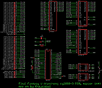
Final Fantasy V (Yancheng cy2000-3 PCB)
| Type | single | | Mapper | 164 | | Original mapper | | | PCB marks | CY2000-3 | | Tags: | | | Uploaded: | 2020-09-14 09:04:37 |
|  |
Elements:
Chip signature:
27F080+6264+62256+EPR1 A2 (not soldered)(93C46)+EPR2 (A3)(93C46)+DIL48
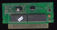
PCB top:
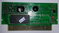
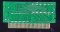
PCB bottom:
Shell top:
No photo
Shell bottom:
No photo
Screenshoots:
No photo
Extra info:
Final Fantasy V (Yancheng cy2000-3 PCB, mapper 164)

Analysis requested by NewRisingSun. This PCB contains:
* 512kB PRG-ROM
* 2kB PRG-RAM
* 93C46 based EEPROM2 PRG-RAM
* 93C46 based EEPROM1 PRG-RAM (unpopulated)
* 8kB blob CHR-RAM
* mapper blob

[url=https://obrazki.elektroda.pl/8105529400_1599518248_org.jpg][img]https://obrazki.elektroda.pl/8105529400_1599518248_thumb.jpg[/img][/url] [url=https://obrazki.elektroda.pl/2170763700_1599518250_org.jpg][img]https://obrazki.elektroda.pl/2170763700_1599518250_thumb.jpg[/img][/url] [url=https://obrazki.elektroda.pl/9627553500_1599518252_org.jpg][img]https://obrazki.elektroda.pl/9627553500_1599518252_thumb.jpg[/img][/url] [url=https://obrazki.elektroda.pl/4056299100_1599518252_org.png][img]https://obrazki.elektroda.pl/4056299100_1599518252_thumb.jpg[/img][/url]

ROM: https://gofile.io/d/fKIT60

[code]
             +--------+
   CPU D5 -> | 01     |
   CPU D4 -> | 02     |
   CPU D3 -> | 03  46 | -- +5V
   CPU D2 <> | 04  45 | <- CPU D6
   CPU D1 -> | 05  44 | <- CPU D7
   CPU D0 -> | 06  43 | <- PPU A13
        ? -> | 07  42 | <- CPU A9
  PPU /RD -> | 08  41 | <- PPU A10
  PPU A3  -> | 09  30 | <- PPU A11
  PPU A12 -> | 10  39 | -> PRG A19
  CHR A12 <- | 11  38 | -> CIR A10
  CHR A3  <- | 12  37 | -> PRG /OE
  PPU A9  -> | 13  36 | -> PRG A18
  PPU A0  -> | 14  35 | -> PRG A17
  WRAM/CE <- | 15  34 | -> PRG A16
  CPU A10 -> | 16  33 | -> PRG A15
  CPU A11 -> | 17  32 | -> PRG A14
  CPU A12 -> | 18  31 | <- CPU A8
 EPR DOUT -> | 19  30 | <- CPU A14
  CPU A13 -> | 20  29 | <- /RESET
       M2 -> | 21  28 | <- CPU /ROMSEL
  EPR DIN <- | 22  27 | -> $5000.4
  EPR CLK <- | 23  26 | -> EPR1 CS
  EPR2 CS <- | 24  25 | -- GND
             +--------+
			 Mapper blob pinout

* While /RESET=0, all bits of internal registers are being cleared (writes are ignored)
* Mapper chip does use CPU R/W, so it cannot distinguish between CPU reads and writes
(all access to $5000/$5100/$5200/$5300 is treated as writes and all access to $5500 as reads)
* Pin 7 is unknown input (internally pulled-up high). Changing its level does not alter
PRG banking behaviour nor its value can be read back in $5500.

----------------------------- Register $5000 (write) -----------------
D~7654 3210
  ---------
  CSQM PPPp
  ||+|-++++- PRG bank (see table below)
  |+-+------ PRG banking mode
  |  +------ value of this bit is also output on pin 27
  |  +------ 1=enables mirroring control by $5300.7, 0=ignores $5300.7 and forces mirroring to V
  +--------- 1 bpp video mode: when PPU A13=0 (pattern table) ...
              0: CHR A3=PPU A3, CHR A12=PPU A12 (disable 1 bpp mode)
              1: CHR A3=PPU A0, CHR A12=PPU A9, both latched on
                 last rise of PPU A13 (enable 1 bpp mode)

S M   QPPPp  | $8000 $C000
-------------+------------
0 0    any   | QPPPp   $1F
             |
1 0 $00..$1B | QPPPp   $1E
1 0 $1C..$1F | QPPPp   $1C
             |
1 1 $00..$0F | PPPp0 PPPp1
1 1 $10..$17 | 0PPPp   $0F
1 1 $18..$1F | 1PPPp   $1F
             |
0 1    any   |   open bus   (See note 1)

Note 1: For that case, PRG A18..A14 are still driven the same way as when S=1 and M=1,
but PRG/CE is always held at 1, so effectively it is open bus for reads from $8000-$ffff
I have no idea what it can be used for.

----------------------------- Register $5100 (write) -----------------
D~7654 3210
  ---------
  .... ...X
          +- PRG A19
----------------------------- Register $5200 (write) -----------------

D~7654 3210
  ---------
  .s.S .C.D
   | |  | +- 93C66 EEPROM1/2 DATA output
   | |  +--- 93C66 EEPROM1/2 CLK output
   | +------ 93C66 EEPROM2 CS output
   +-------- 93C66 EEPROM1 CS output (non populated)

----------------------------- Register $5300 (write) -----------------

D~7654 3210
  ---------
  m... ....
  |
  +--------- Mirroring: 0=H, 1=V


----------------------------- Register $5500 (read) -----------------
D~7654 3210
  ---------
  .... .A..
        |
        |
        +--- 93C66 EEPROM1/2 DATA input (inverted)
[/code]
Comments:
Want to leave a comment?