Basic Educational
| Type | single | | Mapper | | | Original mapper | | | PCB marks | KD-2000 | | Tags: | #reset #big | | Uploaded: | 2021-05-18 01:41:55 |
|  |
Elements:
Chip signature:
74374+74245 (not soldered)(74245)+7420+6116P+74245+6264+27512+27F080+27512 (not soldered)(27512)+16L8+7474
PCB top:
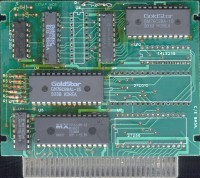
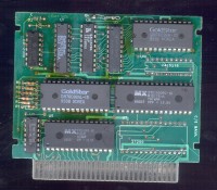
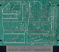
PCB bottom:
Shell top:
Shell bottom:
No photo
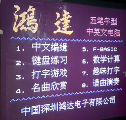
Screenshoots:
Extra info:
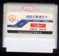
Chinese basic educational computer with EX-RAM
Thanks to MLX & NewRisingSun for letting me test it. Cartridge can operate in one of two modes Originally it would switch on each reset, but for unknown reasons, diode and capacitor, needed for M2 filtering were not installed and instead, additional wires
U9.3 - U9.8
U1.2 - U8.13
U1.15 - U8.12
U9.12 - U4.27
U9.11 - U5.22
were added to make this bizarre circuit that switches between modes every time any write to $8000-$ffff occurs
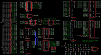
[img]https://obrazki.elektroda.pl/6670000600_1621338471.png[/img]
[b]Mode 0 (PRG_A15=0, so PRG_nA15=1)[/b]
[code]
PRG: |$8000-$ffff |
| 0 |
(first 32 kB of the PRG-ROM chip is used)
CHR: | $0000 | $1000 |
| A+B | A+B |
each 4kB bank points to the same region of CHR memory
* first halves (A) of each tile are in CHR-ROM at $00000-$007FF
* second halves (B) of each tile are in CHR-ROM at $10000-$107FF
PPU ADDRESS SPACE | CHR ROM layout
$0000 -> tile $00 lo | $00000 -> tile $00 lo
$0008 -> tile $00 hi | $00008 -> tile $01 lo
$0010 -> tile $01 lo | ..
$0018 -> tile $01 hi | $007f8 -> tile $ff lo
.. | $00800 \
$0FF0 -> tile $ff lo | > not accessible in this mode
$0FF8 -> tile $ff hi | $0ffff /
--------------------- | $10000 -> tile $00 hi
$1000 -> tile $00 lo | $10008 -> tile $01 hi
$1008 -> tile $00 hi | ..
$1010 -> tile $01 lo | $107f8 -> tile $ff hi
$1018 -> tile $01 hi |
.. |
$1FF0 -> tile $ff lo |
$1FF8 -> tile $ff hi |
The second (unpopulated) CHR-ROM chip (U7) was meant to be enabled when PPU_A12=0 but that would make a conflict with firstgCHR-ROM chip, because it is always enabled at $0000-$1fff
[/code]
-----------
[b]Mode 1 (PRG_A15=1, so PRG_nA15=0)[/b]
[code]
PRG: |$8000-$ffff |
| 1 |
(second 32 kB of the PRG-ROM chip is used)
* $2400-$2800 [..CCCCCC] -> each writes in that region goes to EX-RAM
||||||
++++++- 2k CHR-bank used for the tile (both bitplanes of each sprite are the same)
* then when reading from any of the nametables ($2000, $2400, $2800, $2c00), the same value from EX-RAM is used do determine which CHR-bank should be used for tile
[/code]
PAL equations:
[code]
CHR_A16 = PPU_A3 when PRG_nA15 = '1' else 'Z' --equivalent to ('Z' & !PRG_nA15) | (PRG_nA15 & PPU_A3);
CHR2_nCE = PPU_A12 when PRG_nA15 = '1' else 'Z' --equivalent to ('Z' & !PRG_nA15) | (PRG_nA15 & PPU_A12);
CHR1_nCE = (PPU_A13);
nGNDBUF = 0
EX_nWE = (PPU_nWE);
EX_nCS = (!PPU_nWE & !PPU_A10) | (!PPU_A13);
PPU_nWE PPU_A13 PPU_A10 | EX_nCS
0 * 0 1
0 0 1 1
0 1 1 0
1 0 0 1
1 1 0 0
1 0 1 1
1 1 1 0
EX_CLK = (PPU_nWE & PPU_A13 & !PPU_nRD) | (PPU_A10 & PPU_A13 & !PPU_nRD);
EX_nOC = (PRG_nA15);
[/code]
There is also place for second 74*245 that would drive PPU data bus with zeros, but the PAL lice enabling it is always at zero, so no idea how it oculd be used.Comments:
Want to leave a comment?