Suikoden
Elements:
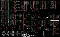
Chip signature:
74157+74273+16L8+27512+16L8+74157+74670+74670+7432+7474+74157+6116P+6264A+6264A+27F080+16L8+74245+74244
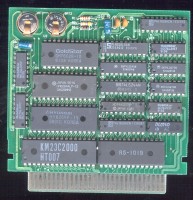
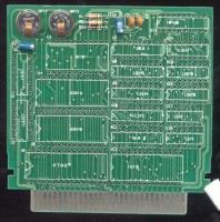
PCB top:
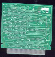
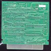
PCB bottom:
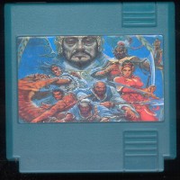
Shell top:
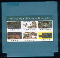
Shell bottom:
Screenshoots:
No photo
Extra info:
U13:
ADR_!CPU!/PPU = (!EXMODE&!M2) | (!EXMODE&!CPU-!ROMSEL!) | (!EXMODE&!CPU-A14) | (!EXMODE&!CPU-A12) | (!EXMODE&!CPU-A10) | (!EXMODE&CPU-R/!W!) | (!EXMODE&CPU-A13);
In VHDL:
ADR_!CPU!/PPU <= '0' when EXMODE='0' and CPU-R/!W!='0' and CPU-A10='1' and CPU-A12='1' and CPU-A13='0' and CPU-A14='1' and CPU-!ROMSEL!='1' and M2='1' else --cpu write at $5400-$5fff
                 '0' when EXMODE='1' else
                 '1';

RAMA_CS = (!REG.2);
In VHDL:
RAMA_CS <= not REG.2;

PRG-A15 = (CPU-A13&CPU-A14) | (REG.2);
In VHDL:
PRG-A15 <= (CPU-A13 and CPU-A14) or (REG.2);

$E000-$FFFF = (CPU-A13&CPU-A14);
In VHDL:
$E000-$FFFF <= '1' when CPU-A13='1' and CPU-A14='1' else '0'

PRG-!CE! = (!REG.7&!CPU-A14) | (CPU-!ROMSEL!);
In VHDL:
PRG-!CE! <= '1' when REG.7='0' and CPU-A14='0' else CPU-!ROMSEL!;

RAM_!CS! = (!CPU-A13&CPU-!ROMSEL!) | (REG.7&!CPU-!ROMSEL!) | (CPU-!ROMSEL!&!M2) | (CPU-A14&!CPU-!ROMSEL!) | (!CPU-A14&CPU-!ROMSEL!);
In VHDL:
RAM_!CS! <= '0' when CPU-A13='1' AND CPU-A14='1' AND CPU-!ROMSEL='1' AND M2='1' else
            '0' when REG.7='0' AND CPU-A14='0' and CPU-!ROMSEL!='0' else
            '1'

 REG.7 | CPU-A13 | CPU-A14 | CPU-!ROMSEL! | M2 || RAM_!CS!  |
     0 |       0 |       0 |            0 |  0 ||        0  | <--- 8000$-$bfff and REG.7=0
     0 |       0 |       0 |            0 |  1 ||        0  | <--- 8000$-$bfff and REG.7=0
     0 |       1 |       0 |            0 |  0 ||        0  | <--- 8000$-$bfff and REG.7=0
     0 |       1 |       0 |            0 |  1 ||        0  | <--- 8000$-$bfff and REG.7=0
     0 |       1 |       1 |            1 |  1 ||        0  | <-6000-$7fff
     1 |       1 |       1 |            1 |  1 ||        0  | <-6000-$7fff

!$4400-$4FFF! = (!M2) | (!CPU-!ROMSEL!) | (!CPU-A14) | (!CPU-A10) | (CPU-A12) | (CPU-A13);
In VHDL:
!$4400-$4FFF! <= '0' when M2='1' and CPU-!ROMSEL!='1' and CPU-A14='1' and CPU-A10='1' and CPU-A12='0' and CPU-A13='0' else '1';

!$5400-$5FFF! = (!M2) | (!CPU-!ROMSEL!) | (!CPU-A14) | (!CPU-A12) | (!CPU-A10) | (CPU-A13);
In VHDL:
!$5400-$5FFF! <= '0' when M2='1' and CPU-!ROMSEL!='1' and CPU-A14='1' and CPU_A12='1' and CPU-A10='1' and CPU=A13=0 else '1';

--------------------------------------------------------------------------------------------
U11:

O0 = (!I8);
In VHDL:
O0 <= not I8; --but it is unwired

O1 = (I11); --so O1 acts as an input but seems to not have influence to any output)

EX-D5 = (PA12L & PPU-!RD! & !PPU-A13);
In VHDL:
EX-D5 <= '1' when PA12L='1' and PPU-!RD!='1' and PPU-A13='0' else '0'

!PPU_FILL! = (!PPU-A13) | (!PPU-A6) | (!PPU-A7) | (!PPU-A8) | (!PPU-A9) | (PPU-!RD!);
In VHDL:
!PPU_FILL! <= (not PPU-A13) or (not PPU-A6) or (not PPU-A7) or (not PPU-A8) or (not PPU-A9) or (PPU-!RD!);

CIRAM-!CS! = (PPU-A9 & PPU-A8 & PPU-A7 & PPU-A6 & !PPU-!RD!) | (!PPU-A13);
In VHDL:
CIRAM-!CS! <= (PPU-A9 and PPU-A8 and PPU-A7 and PPU-A6 and !PPU-!RD!) or (not PPU-A13);

CHR-!CE! = (PPU-!RD!) | (PPU-A13);
In VHDL:
CHR-!CE! <= (PPU-!RD!) or (PPU-A13);

!CHR_CLR! = (PPU-A12) | (PPU-A13);
In VHDL:
!CHR_CLR! <= (PPU-A12) or (PPU-A13);

CHR_CLK = (PPU-!RD!&PPU-A13);
In VHDL:
CHR_CLK <= (PPU-!RD! and PPU-A13);

--------------------------------------------------------------------------------------------
U7:
EX-!WE! = (EX-R/!W/) | (CPU-R/!W!);
In VHDL:
EX-!WE! <= (EX-R/!W/) or (CPU-R/!W!);

CIRAM-A10 = Non-combinatorial
O2 = Non-combinatorial
O3 = Non-combinatorial
O4 = Non-combinatorial
EX-!OE! = Non-combinatorial
EXMODE = Non-combinatorial

In VHDL:
O2 <= D0 when CPU-A5='1' and CPU-A4='0' and CPU-A11='1' and CPU-R/!W!='0' and !$4400-$4FFF!='0'; //latch

O3 <= D2 when CPU-A5='1' and CPU-A4='0' and CPU-A11='1' and CPU-R/!W!='0' and !$4400-$4FFF!='0'; //latch

O4 <= D0 when CPU-A5='1' and CPU-A4='1' and CPU-A11='1' and CPU-R/!W!='0' and !$4400-$4FFF!='0'; //latch

EXMODE <= D1 when CPU-A5='1' and CPU-A4='1'  and CPU-A11='1' and CPU-R/!W!='0' and !$4400-$4FFF!='0'; //latch

EX-!OE! <= not (EXMODE or O4)

CIRAM-A10 <= '0' when O3='0' and O2='0' else
            not PPU-A10 when O3='0' and O2='1' else
            PPU-A10 when O3='1' and O2='0' else
            '1';

!WR_$4C00! = (!CPU-A11) | (!$4400-$4FFF!) | (CPU-R/!W!) | (CPU-A5) | (CPU-A4);  !WR_$4C00! , mask: $FC30
In VHDL:
!WR_$4C00! <= (not CPU-A11) or (!$4400-$4FFF!) or (CPU-R/!W!) or (CPU-A5) or (CPU-A4);  !WR_$4C00! , mask: $FC30


Those latched regs summary:
$4c00 .... .... (no effect?)
$4c10 .... .... (no effect?)
$4c20 .... .m.m
			| |
			+++-- mirroring (source of CIR10): 0: GND, 1: not PA10, 2: PA10, 3: VCC

$4c30 .... ..ee
             ||
			 ++-- value of EX-!OE! to be latched (enable reading from EX-ram: 0=disable=VCC, 1..3:enable=GND)
			 +--- value of EXMODE to be latched

--------------------------------------------------------------------
Hardware: 256K PRG-ROM
          8KB  PRG-RAM battery backed (6264A)
		  8KB  PRG-RAM not backed (6264B)
		  64KB CHR-ROM
		  1KB  EX-RAM (can be used by CPU & PPU)

Quirks:
* Data bit 5 of EX-RAM is not wired to anything

CPU memory map:
$4400-$47ff: registers
$4c00-$4fff: registers (mirror)

PPU memory map:
$0000-$0fff: 4KB CHR-ROM bank
$1000-$1fff: 4KB CHR-ROM bank
0b1xxx1111xxxxxx: fill mode

$5400-$57ff: EXRAM
$5c00-$5fff: EXRAM (mirror)
$6000-$7fff: RAM (controlled by $4c03)
$8000-$9fff: ROM or RAM (controlled by $4c00)
$a000-$bfff: ROM or RAM (controlled by $4c01)
$c000-$dfff: ROM (controlled by $4c02)
$e000-$ffff: ROM (hardwired to last bank)


[r..p pppp] $4c00 (mask: $fc33)
 |  | ||||
 |  +-++++- select 8kB ROM bank at $8000-$9fff (ignored when RAM is selected)
 |     +--- select RAM chip 0=6264A, 1=6264B   (ignored when ROM is selected)
 +--------- 0: select RAM, 1:select ROM

[r..p pppp] $4c01 (mask: $fc33)
 |  | ||||
 |  +-++++- select 8kB ROM bank at $a000-$bfff (ignored when RAM is selected)
 |     +--- select RAM chip 0=6264A, 1=6264B   (ignored when ROM is selected)
 +--------- 0: select RAM, 1:select ROM

[...p pppp] $4c02 (mask: $fc33)
    | ||||
    +-++++- select 8kB ROM bank at $c000-$dfff

[.... .p..] $4c03 (mask: $fc33)
       |
       +--- select RAM chip for $6000-$7fff: 0=6264A, 1=6264B

[.... .m.m] $4c20 (mask: $fc30)
       | |
       +++-- Mirroring - source of CIRAM-A10: 0=GND, 1=not PA10, 2=PA10, 3=VCC

[.... ..ee] $4c30 (mask: $fc30)
        ||
        ++-- controls EX-RAM !OE line (0:disable, 1..3:enable)
        +--- controls what is connected to EX-RAM address bus,!WE and !CS:
		     0=CPU bus when CPU writes at $5400-$57ff/$5c00-$5fff, otherwise PPU bus)
			 1=always CPU bus

EX-RAM behaviour:
CPU has two windows ($5400-$57ff and $5c00-$5fff) to read/write to EX-RAM memory.
The behaviour of EX-RAM depends of how $4c30 bits are set.
CPU can always write to EX RAM (and those write cycles have priority over any other EXRAM activity)

0: reading from EXRAM (by CPU/PPU) returns open bus; CPU can write to EX-RAM.
1: reading EXRAM by CPU returns open bus; CPU can write to EX-RAM; PPU can read EX-RAM
2-3: CPU can read & write to EX-RAM, PPU cannot read from it.
Comments:
Want to leave a comment?