Can you help getting more info about those carts?
| Unique visits: 7975 Can you help getting more info about those carts? |
|  |
| Name | Value |
|---|---|
| IC1 | 6264A |
| IC2 | 27512 |
| IC3 | KS204-MMC3 |
| IC4 | 6264A |
| IC5 | 74138 |
| IC6 | 7408 |
| IC7 | 7486 |
| C1 | 10u |
| C2 | - |
| C3 | - |
| C4 | - |
| CART1 | FAMICOM_CART |
| R1 | 100R |
| R2 | 4,7k |
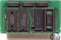
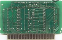
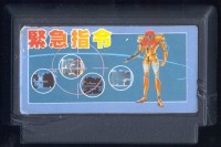
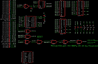
Kaiser KS 204 chip
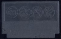
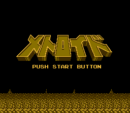
I finally was able to obtain one game with KS 204 Kaiser chip and analyze it.
[url=https://obrazki.elektroda.pl/1203224600_1567180289.jpg][img]https://obrazki.elektroda.pl/1203224600_1567180289_thumb.jpg[/img][/url] [url=https://obrazki.elektroda.pl/2811728300_1567180291.jpg][img]https://obrazki.elektroda.pl/2811728300_1567180291_thumb.jpg[/img][/url] [url=https://obrazki.elektroda.pl/9834154900_1567180316.jpg][img]https://obrazki.elektroda.pl/9834154900_1567180316_thumb.jpg[/img][/url] [url=https://obrazki.elektroda.pl/7932394000_1567180318.jpg][img]https://obrazki.elektroda.pl/7932394000_1567180318_thumb.jpg[/img][/url] [url=https://obrazki.elektroda.pl/1499492800_1567180319.png][img]https://obrazki.elektroda.pl/1499492800_1567180319_thumb.jpg[/img][/url]
The KS204 chip is nothing more but a Kaiser clone of Tengen MIMIC-1 MMC3 predessor ([url=http://wiki.nesdev.com/w/index.php/INES_Mapper_206]INES Mapper 206[/url]), known also as [url=http://wiki.nesdev.com/w/index.php/Namcot_108_family_pinout]NTDEC 8701[/url].
The only difference is lack of PRG/CE pin (instead, external RESET is present) and shuffled pinout.
[code]
.--\/--.
M2 -> |01 28| -- +5V
CPU R/!W -> |02 27| <- RESET
CPU A14 -> |03 26| <- CPU D3
CPU A13 -> |04 25| -> CHR A15
CPU D1 -> |05 24| -> CHR A14
CPU D0 -> |06 23| -> CHR A13
CPU !RMS -> |07 22| -> CHR A12
CPU D4 -> |08 21| -> CHR A11
CPU A0 -> |09 20| -> CHR A10
PRG A16 <- |10 19| <- CPU D5
PRG A15 <- |11 18| <- PPU A12
PRG A14 <- |12 17| <- PPU A11
PRG A13 <- |13 16| <- PPU A10
GND -- |14 15| <- CPU D2
`------'
KS 204
[/code]
Details:
* Latching values into registers occurs on the rising edge of its decoding signal, for example register $8000 has decoding signal like:
CLK <= '0' when /ROMSEL = 0 and M2 = 1 and R/W = 0 and A1 = 0 and A14 = 0 and A13 = 0 else '1'
This can be precisely simulated using 74138+74574:
[url=https://obrazki.elektroda.pl/2030486500_1567158285.png][img]https://obrazki.elektroda.pl/2030486500_1567158285_thumb.jpg[/img][/url]
* PRG bank address lines does not take CPU-!ROMSEL into account so $0000-$7fff mirrors $8000-$ffff (important when external logic enables ROM under $8000)
However, the "Metroid [FDS port], PCB: KS-7037)" games that uses it, connects it differently, which results in the following register order:
[code]
$8000.R2 [.......I] - nametable for $2000
$8000.R3 [.......J] - nametable for $2800
$8000.R4 [.......K] - nametable for $2400
$8000.R5 [.......L] - nametable for $2c00
$8001.R6 [....ABCD]
$8001.R7 [....EFGH]
$6000 $7000 $8000 $9000 $a000 $b000 $c000 $d000 $e000 $f000
----- ----- ----- ----- ----- ----- ----- ----- ----- -----
RAM ROM ROM ROM ROM RAM ROM ROM ROM ROM
0 11111 ABCD0 ABCD1 01100 1 EFGH0 EFGH1 01110 01111 <- 4 kiB Bank
^ ^ ^ ^
+-----+-----------------+-----+------------------- those bits are inverted
Writing to $7000-$7fff can cause bus-conflicts (ROM is enabled at that region during writes),
while writing to other regions doesn't.
The UNL-KS7037 FCEUX mapper implementation does not invert those bits but that's because
my implementation respects the PRG-A16 address line (just like the EPROM was dumped first and then
mapper was implemented to match it)
[/code]Comments: