32 in 1
Elements:
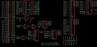
Chip signature:
27F080+27F080+AX5202P(MMC3)+6264+74153+74174+74157+7402
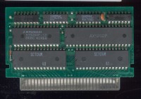
PCB top:
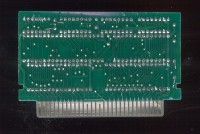
PCB bottom:
Shell top:

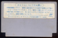
Shell bottom:
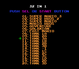
Screenshoots:
Extra info:
The reset detection circuit causes the reset to trigger only if M2 is high (or high impedance) for long period of time.
M2 --|<|--+
GND--100n-+---)NOR)--/RESET

This is different comparing to most reset circuits, where it trigger if M2 is low (or high impedance) for long periods of time

VCC----R--+
M2 --|>|--+
GND----C--+----------/RESET


There is one additional register at $6000-$7fff, cleared on power/reset.
READ or WRITE cycle at $6000-$7fff causes latching of address bits.
(MMC3's $A001 reg must allow for such access: %1xxxxxxx for reads, %10000000 for writes)

   fedcba9876543210
A~[011.......mabpqr]
             |||+++-- PRG A16..14 (see bellow)
             |||++--- PRG mode (00=16k, 01/10/11=32k)
             ||+----- PRG A17 (see bellow)
             |+------ PRG-A18, CHR-A18
             |+------ 0: PRG-A17=CHR-A17=b, 1:PRG-A17=CHR-A17=MMC3-PRG-A17
             +------- banking mode:
             |          1=PRG-A16..13 comes from MMC3
             |          0=PRG-A16=p, PRG-A15=q, PRG-A14=r when p=0 & q=0 else CPU-A14, PRG-A13 = CPU-A13
             +------- 1=future writes to this register are ignored (until restart)

CHR-A16..CHR-A17 always comes from MMC3's CHR

Or in detailed form:

 # - MMC3's PRG bit for the corresponding bank
-----+--------- CPU MAP ----------
mapq |  $8000  $a000  $c000  $e000
0000 | 0b00r0 0b00r1 0b00r0 0b00r1     ;NROM 16kB
00** | 0bpq00 0bpq01 0bpq10 0bpq11     ;NROM 32kB
0100 | 1#00r0 1#00r1 1#00r0 1#00r1
01** | 1#pq00 1#pq01 a#pq10 1#pq11
10** | 0b#### 0b#### 0b#### 0b####     ;MMC3 128kB PRG -> SMB2
11** | 1##### 1##### 1##### 1#####     ;MMC3 256kB PRG -> SMB3
                            ++++++- PRG A18, A17, A16, A15, A14, A13

PPU MAP:
----+----------- PPU MAP ---------
a   | $0000     | $0400 | $0800 | $0c00 | $1000 | $1400 | $1800 | $1c00
0   | 0b@@@@@@@	|  <--  |  <--  |  <--  |  <--- |  <--  |  <--  |  <--
1   | 1#@@@@@@@ |  <--  |  <--  |  <--  |  <--  |  <--  |  <--  |  <--
      +++++++++- CHR A18, A17, A16, A15, A14, A13, A12, A11, A10
@ - MMC3's CHR bit for the corresponding bank
# - MMC3's PRG A17

When a=1, CHR A17 is dependent on the PRG-A17 from MMC3, which is quite strange because this would change the CHR-BANK depending on if the cpu is executing code from fixed bank or not. But this does not matter because third and fourth chunk of the ROM is identical

--
Dumping this game without de-soldering ROMS and preserving the order of byes as it is burned into ROM is quite tricky, because it involves going through different PRG banking modes to cover all ROM adresses:

//PRG DUMPING
cpu_write(0xa001, new byte[] { 0x80 }); //enable access to the register
int m = 0; int a = 0;
for (int b = 0; b < 2; ++b) {
	for (int pq = 0; pq < 4; ++pq) {
		if (pq == 0) {
			for (int r = 0; r < 2; ++r) {
				cpu_read(0x6000 | m << 5 | a << 4 | b << 3 | pq << 1 | r, 1);
				cpuRead(0x8000, 0x9fff);
				cpuRead(0xa000, 0xbfff);
			}
		}
		else {
			cpu_read(0x6000 | m << 5 | a << 4 | b << 3 | pq << 1, 1);
			cpuRead(0x8000, 0x9fff);
			cpuRead(0xa000, 0xbfff);
			cpuRead(0xc000, 0xdfff);
			cpuRead(0xe000, 0xffff);
		}
	}
}
m = 1;
a = 1;
cpu_read(0x6000 | m << 5 | a << 4, 1);
for (int bank = 0; bank < 32; ++bank) {
	cpu_write(0x8000, new byte[] {6});
	cpu_write(0x8001, new byte[] { (byte)bank });
	cpuRead(0x8000, 0x9fff);
}


//CHR DUMPING
cpu_write(0xa001, new byte[] { 0x80 });
for (int a = 0; a < 2; ++a) {
	for (int b = 0; b < 2; ++b) {
		if (a == 0) {
			cpu_read(0x6000 | a << 4 | b << 3, 1);
		}
		else {
			cpu_read(0x6000 | a << 4, 1);
			cpu_write(0x8000, new byte[] { (byte)6 });
			cpu_write(0x8001, new byte[] { (byte)(b << 4) });
		}

		for (int i = 0; i < 128; ++i) {
			cpu_write(0x8000, new byte[] {2});
			cpu_write(0x8001, new byte[] { (byte)i });
			ppuRead(0x1000, 0x13ff);
		}

	}
}
Comments:
Want to leave a comment?