168 in 1
Elements:
Chip signature:
27F080+6264A+7402 (not present)(7402)+DIL28+74157
PCB top:
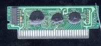
PCB bottom:

Shell top:
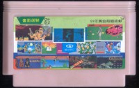
Shell bottom:

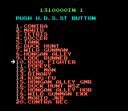
Screenshoots:
Extra info:
Main register. Bus conflicts. On power up + reset all bits are cleared.
   fedcba9876543210     76543210
A~[1.w..ybPxPPpppmv] D~[........]
     |  |||||||||||
     |  ||||||||||+-------------- mode (0=16K, 1=32K)
     |  |||||||||+--------------- mirroring (0=V, 1=H)
     |  ||||||+++---------------- inner PRG bank
     |  |||+||------------------- banking mode (0=UNROM, 1=NROM) & chr write pritection (0=off, 1=on)
     |  ||+-++------------------- outer PRG bank
     |  |+----------------------- PRG bank used for UNROM mode
     |  +------------------------ PRG chip selection (*)
     +--------------------------- Write protection of bits d/a/9/8/7/6 (0=off, 1=on)

xv |  $8000 |  $c000
0* | yPPPppp | yPPPbbb
10 | yPPPppp | yPPPppp
11 | yPPPpp0 | yPPPpp1

`y` bit for emulation purposes can be treaten as highest (A20) PRG bank bit. However, hardware implementation varies:
1) There are two PRG ROM chips and this bit it used to switch between two roms: 1=1MB chip, 0=128k chip (cart: 190 in 1);
2) There is one 1MB PRG ROM chip and this bit is used to switch what is connected to lowest PRG_A lines
  - PRG-A[3..0]: 0=CPU-A[3..0], 1=[0,1,1,1] (carts: 3000 in 1, 400 in 1)
  - PRG-A[4..0]: 0=CPU-A[4..0], 1=[0,1,1,0,1] (carts: 168 in 1)

dumping script:
for (int c = 0; c < 2; ++c) {
	for (int i = 0; i < (c == 0 ? 128 : 1024) / 16; ++i) {
		cpuWrite(0x8000 | ((i & 31) << 2) | (((i >> 5) & 1) << 7) | (c << (0xa)), 0);
		cpuRead(0x8000, 0xBfff);
	}
}
Comments:
Want to leave a comment?