1KK000 in 1
| Type | multi | | Mapper | 362 | | Original mapper | 0 | | PCB marks | RM2M1M | | Tags: | #iii | | Uploaded: | 2017-07-28 01:10:24 |
|  |
Elements:
| Name | Value |
|---|
| IC1 | 27F080 |
| IC2 | 27512 |
| U3 | 74273 |
| U4 | 16L8 |
| U5 | -(DIL14) |
| C1 | 100n |
| C2 | 10n |
| CART1 | FAMICOM_CART |
| D1 | DIODE |
| D2 | DIODE |
| D3 | DIODE |
| J1 | JP1E |
| J2 | JP1E |
| J3 | JP1E |
| J4 | JP1E |
| R1 | 2.2k |
| R2 | - |
| R3 | - |
| R4 | - |
| R5 | - |
| R6 | 2.2k |
Chip signature:
27F080+27512+74273+16L8+-(DIL14)
PCB top:
PCB bottom:
Shell top:
No photo
Shell bottom:
No photo
Screenshoots:
Extra info:
Reverse engineering funny multi-game cartridge
I got Rinco famiclone (which looks just like Famicom) to fix it. It has one additional 60 pin cartridge socket underneath with multi-game cartridge inserted. I decided to reverse-engineer it because it looks funny (PAL, so many diodes and some mysterious pads with missing chips & resistors)
[url=http://obrazki.elektroda.pl/1674260900_1501282772.jpg][img]http://obrazki.elektroda.pl/1674260900_1501282772_thumb.jpg[/img][/url]
The cartridge was probably projectted to be put in two-slot consoles, because it is really narrow (nothing to lock against clips in cartridge shell) and was done on 1.5 mm laminate - requires so much force to put it inside.
I dumped the menu (CPU $8000-$FFFF + PPU $0000-$1FFF), which can be done with help of kazzo to almost any multicart cartridge without knowledge how it works - except those which start messing with banks at startup.
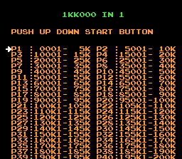
Cartridge contains 200 000 games, but in fact, only: Mario, Lunar ball, Duck Hunt, Wild gunman, Hogans Alley, Bomber man, Tank, Sky destroyer, Binary land, Ice climber. Programmers divided the menu into 1-5000, 5001-10000, etc for easier navigation.
[url=http://obrazki.elektroda.pl/4233306400_1501283468.png][img]http://obrazki.elektroda.pl/4233306400_1501283468_thumb.jpg[/img][/url] [url=http://obrazki.elektroda.pl/4565223800_1501283468.png][img]http://obrazki.elektroda.pl/4565223800_1501283468_thumb.jpg[/img][/url] [url=http://obrazki.elektroda.pl/9240226500_1501283469.png][img]http://obrazki.elektroda.pl/9240226500_1501283469_thumb.jpg[/img][/url]
First i desoldered chips and rev-ed all tracks
[url=http://obrazki.elektroda.pl/2676737600_1501283524.jpg][img]http://obrazki.elektroda.pl/2676737600_1501283524_thumb.jpg[/img][/url] [url=http://obrazki.elektroda.pl/6811442900_1501283526.jpg][img]http://obrazki.elektroda.pl/6811442900_1501283526_thumb.jpg[/img][/url]
Those glob-tobs have pins in almost same order like ordinary ROMs:
[url=http://obrazki.elektroda.pl/6389913900_1501283855.jpg][img]http://obrazki.elektroda.pl/6389913900_1501283855_thumb.jpg[/img][/url] [url=http://obrazki.elektroda.pl/1506105800_1501283857.jpg][img]http://obrazki.elektroda.pl/1506105800_1501283857_thumb.jpg[/img][/url]
PRG-ROM is 256k, CHR-ROM is 128 kB. CHR-ROM has only one chip enable line.
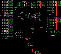
Then I rev-ed schematics:
[url=http://obrazki.elektroda.pl/7181911200_1501285358.png][img]http://obrazki.elektroda.pl/7181911200_1501285358_thumb.jpg[/img][/url]
Some notes:
* There is 74273 8 bit latch (adress bits A0-A7 are latched, but A4 & A5 are not used)
* ROM is not turned off during writes at $8000-$FFFF (bus conflicts),
* There is R-C-D reset circuitry which sets latch's bits to 0 on startup,
* Two diodes + resistors were used as poor man's OR gate (ORing PPU-A13 & PPU-!RD to feed the result into CHR-ROM's !CE),
* PAL16L8's is configured to serve as 12 input & 6 output combinational logic.
Then I dumped the PAL to binary using my home-made flash reader.
Then I wrote simple program to convert the binary file into espresso text description:
[code]
.i 12
.o 6
.ilb PPU-A11 PPU-A10 REG.A7 REG.A6 CPU-A14 CPU-A13 CPU-A12 REG.A2 REG.A1 REG.A0 CPU-!ROMSEL! CPU-R/!W!
.ob REG.WR PRG-A14 PRG-A15 PRG-A16 BUF-!OE! CIRAM-A10
000000000000 000010
000000000001 000010
000000000010 000010
000000000011 000010
000000000100 010010
000000000101 010010
000000000110 010010
000000000111 010010
...
[/code]
Then I ran espresso on this file to generate logic formulas for each output:
[code]
REG.WR = (CPU-A14 & not CPU-A13 & CPU-A12 & CPU-!ROMSEL! & not CPU-R/!W!);
PRG-A14 = (not REG.A6 & CPU-A14 & not REG.A1) | (not REG.A6 & CPU-A14 & not REG.A2) | (REG.A0);
PRG-A15 = (not REG.A6 & REG.A2 & REG.A0) | (not REG.A6 & CPU-A14 & not REG.A2) | (REG.A1);
PRG-A16 = (not REG.A6 & CPU-A14 & notREG.A2) | (REG.A2);
BUF-!OE! = (CPU-A14 & not CPU-A13 & CPU-A12 & CPU-!ROMSEL! & not CPU-R/!W!) | (not CPU-!ROMSEL!) | (notCPU-A12) | (CPU-A13) | (not CPU-A14);
CIRAM-A10 = (PPU-A10 & not REG.A7) | (PPU-A11 & REG.A7);
[/code]
Data is latched on rising edge of REG.WR signal, which corresponds to writes at $5000-$5FFF (beginning of cycle) or $D000-$DFFF (end of cycle). In fact, first region is used because it does not produce bus conflicts with ROM.
Generally:
* PRG-A14 <- A0, PRG-A15 <- A1, PRG-A16 <- A2, PRG-A17 <= A3 (at $8000-$b000),
* A6 controls 16 KB / 32 KB banking mode,
* at $c000-$ffff there is some magic,
* A7 controls mirroring
[b]Mysterious DIL14 chip, resistors and jumpers[/b]
In those mysterious 14 pads probably 74125 tri state buffer should be placed:
[url=http://obrazki.elektroda.pl/2821776800_1501285500.png][img]http://obrazki.elektroda.pl/2821776800_1501285500_thumb.jpg[/img][/url] [url=http://obrazki.elektroda.pl/6852534800_1501285591.gif][img]http://obrazki.elektroda.pl/6852534800_1501285591_thumb.jpg[/img][/url]
Its four inputs are combination of GND/VCC (according to jumpers), which are placed on D0-D3 bus when BUF_!OE goes low, which corresponds to reading from $5000-$5FFF. Probably that could be used for reading some magic value and displaying different game sets, based on that (manufacturer could produce just one type of PCB with same glop-tops and create pseudo-different cartridges according to jumpers)
Kazzo script for dumping whole set would be:
for (a = 0x5000; a < 0x5010; ++a) {
cpu_w(a, 0x00);
cpu_r(0x8000, 0xbfff);
ppu_r(0x0000, 0x1fff);
}
During whole operation, m2 must have 1.7 MHz clock, otherwise register will reset.Comments:
Want to leave a comment?