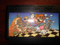
Super Mario Bros 3 (KS202)
| Type | single | | Mapper | 56 | | Original mapper | 4 | | PCB marks | | | Tags: | #smb3 | | Uploaded: | 2019-09-22 11:08:39 |
|  |
Elements:
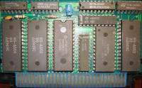
Chip signature:
R5-A004(27512)+16L8+6116L24+R5-A002(27512)+6264+R5-A003(27512)+74670+74157+74240+7408+KS202(DIL20)
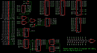
PCB top:
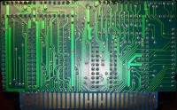
PCB bottom:
Shell top:
Shell bottom:
No photo
Screenshoots:

Extra info:
http://www.mediafire.com/file/4dc6o4q8v68378u/assembler_backup.7z/file

http://assemblergames.com/threads/any-information-on-this-super-mario-bros-3-famicom-cart.36468

Oh thank you, that helped a lot!

KS202's pinout seems to be:
[code]
                .--\/--.
     CPU-A12 -> |01  20| -> WRAM-/CE
     CPU-A13 -> |02  19| <- CPU-D3
     CPU-A14 -> |03  18| <- CPU-R/W
         VCC -- |04  17| <- CPU-D0
          M2 -> |05  16| <- CPU-D1
     PRG-A14 <- |06  15| <- CPU-D2
     PRG-A13 <- |07  14| -- GND
     PRG-A15 <- |08  13| <- CPU-/ROMSEL
     PRG-A16 <- |09  12| <- RESET
     PRG-/CE <- |10  11| -> /IRQ
                `------'
[/code]
How it function is unknown, but surely it can only be responsible for PRG banking (up to 128K), IRQ (probably counting CPU cycles), generating WRAM and PRG /CE signal (the last one is not used).

PAL pinout seems to be:
[code]
                 .--\/--.
     CPU-A10  -> |01  20| -- VCC
     CPU-A11  -> |02  19| -> CIRAM-A10
CPU-A12&13&14 -> |03  18| -> PPU-A13
  CPU-/ROMSEL -> |04  17| -> MUX-RD/WR
  REG1-D4 (*) -> |05  16| -> CHR-/CE
      CPU-R/W -> |06  15| -> PRG2-/CE
       CPU-D0 <- |07  14| -> PRG1-/CE
      PPU-A10 -> |08  13| n/c (internal feedback)
      PPU-A11 -> |09  12| -> REG1-/GW (*)
          GND -- |10  11| <- PPU-/RD (filtered ??)
                 `------'
[/code]
Its role is to:
* Add PRG-A17, stored in 74670 (*) and generate PRG1/CE, PRG2/CE
* Generate CHR /CE
* Generate CIRAM-A10 (internally latched D0),
* Generate signal controlling the 6116+74240+74157 CHR-ROM register

Doubts/notes:
* I am not sure which bit is used as PRG-A17 (logically should be CPU-D4, but the via under PRG-ROM can go to anything, maybe even address bit)
* Cant determine register addresses for PRG/CHR banking and IRQ
* 8x1k CHR-banks, not 2x2k+4x1k like in MMC3

[url=https://obrazki.elektroda.pl/6881108100_1569235071.png][img]https://obrazki.elektroda.pl/6881108100_1569235071_thumb.jpg[/img][/url] [url=https://obrazki.elektroda.pl/3931432300_1569235077.png][img]https://obrazki.elektroda.pl/3931432300_1569235077_thumb.jpg[/img][/url] [url=https://obrazki.elektroda.pl/3003008000_1569235077.png][img]https://obrazki.elektroda.pl/3003008000_1569235077_thumb.jpg[/img][/url]

---

Oh, I found this ROM and a [url=https://problemkaputt.de/everynes.htm#mapper56piratesmb3]description[/url] of the mapper, other source claims this mapper is also called KS7022C.

The above mapper description does not quite match the hardware (for example: F000/F001/F003 select banks while KS202 does not have A0/A1 routed). After more analysis of the ROM it turned out that the KS202 chip has 8 registers ((mask $F000):
[code]
*$8000 [....IIII] - set bits 3-0 of 16 bit IRQ counter
*$9000 [....IIII] - set bits 7-4 of 16 bit IRQ counter
*$a000 [....IIII] - set bits 11-8 of 16 bit IRQ counter
*$b000 [....IIII] - set bits 15-12 of 16 bit IRQ counter
*$c000 [.......E] - irq enable (FF, disable: 00), probably only bit0 of written value maters
*$d000 [........] - any write acknowledges pending IRQ
*$e000 [......RR] - set register number to update on writing to $f000
*$f000 [....PPPP] - set PRG bank:
                       00 -> no effect
                       01 -> $8000-$9fff
                       10 -> $a000-$bfff
                       11 -> $c000-$dfff
                       ($e000-$ffff always points to bank 15)
[/code]
The value of each nibble of 16 bit counter is manipulated directly. It counts up and when overflows - IRQ is generated (if it it enabled).

Independently of the KS202, there is PAL16L8 + other logic (mask $FC00) with its job:
[code]
mask $FC03:
  *$f000 [...P....] - select PRG-A17 (bit 5) for $8000-$9fff (1 on powerup)
  *$f001 [...P....] - select PRG-A17 (bit 5) for $a000-$bfff (1 on powerup)
  *$f002 [...P....] - select PRG-A17 (bit 5) for $c000-$dfff (1 on powerup)
  *$f003 [...P....] - select PRG-A17 (bit 5) for $e000-$ffff (1 on powerup)
mask $FC00:
  *$f800 [.......m] - select mirroring (0=H, 1=V)
mask $FC07:
  *$fc00 [.CCCCCCC] - select 1kB CHR for $0000-$03ff
  *$fc01 [.CCCCCCC] - select 1kB CHR for $0400-$07ff
  *$fc02 [.CCCCCCC] - select 1kB CHR for $0800-$0bff
  *$fc03 [.CCCCCCC] - select 1kB CHR for $0c00-$0fff
  *$fc04 [.CCCCCCC] - select 1kB CHR for $1000-$13ff
  *$fc05 [.CCCCCCC] - select 1kB CHR for $1400-$17ff
  *$fc06 [.CCCCCCC] - select 1kB CHR for $1800-$1bff
  *$fc07 [.CCCCCCC] - select 1kB CHR for $1c00-$1fff
[/code]

* The game relies on fact that 74680 is initialized to 1 on powerup
* Writing to any of PAL regs also trigger write to KS202

e:\Pulpit\projekty\elektronika\6502, nes, pegasus\cart-RevEn,Naprawa\ks202 super mario bros 3\rom\Super Mario Bros 3 [p2][!] (Apply over Super Mario Bros 3 (J).nes).IPS

--
So the PAL equations are probably:

--or opposite
PRG1_nCE <= 0 when REG1_D4=0 and CPU_nROMSEL=0 and CPU_RnW=1 else 1
PRG2_nCE <= 0 when REG1_D4=1 and CPU_nROMSEL=0 and CPU_RnW=1 else 1

--no idea how it could ever work, cause every edge on PPU_nRD cause just short spike
CHR_nCE <= 0 when PPU_A13=0 and PPU_nRD=0 else 1

REG1_nGW <= 0 when CPU_nROMSEL=0 and CPU_RnW=0 and CPU_A14&A13&A12=1 and CPU_A11=0 and CPU_A10=0 else 1

O1 <= CPU_D0 when  CPU_nROMSEL=0 and CPU_RnW=0 and CPU_A14&A13&A12=1 and CPU_A11=1 and CPU_A10=0 --latch

--not sure if CPU_nROMSEL is taken into account because 74157 already uses it
MUX_RDnWR <= 0 when CPU_nROMSEL=0 and CPU_RnW=0 and CPU_A14&A13&A12=1 and CPU_A11=1 and CPU_A10=1 else 1

CIRAM_A10 <= PPU_A10 when O1=1 else PPU_A11
Comments:
Want to leave a comment?