http://forums.nesdev.com/viewtopic.php?f=3&t=18723
https://wiki.nesdev.com/w/index.php/NES_2.0_Mapper_538
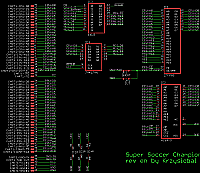
[code]
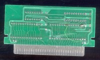
$C000-$DFFF: [....PPPP] (mask: $E000)
||||
++++- Bank value (unspecified on powerup)
Bank | 0 1 2 3 4 5 6 7 8 9 a b c d e f
------+---------------------------------
$6000 | 1 1 3 3 5 5 7 7 9 9 b b d d f f
$8000 | 0 a 2 a 4 a 6 a 8 8 a a c c e e
$a000 | d d d d d d d d d d d d d d d d
$c000 | e e e e e e e e e e e e e e e e
$e000 | f f f f f f f f f f f f f f f f
PAL equations:
[code]
nREGWR = (!M2) | (!CPU_A14) | (CPU_A13) | (CPU_nROMSEL) | (CPU_R_nW);
O1 = (!CPU_A13 & !CPU_A14) | (CPU_nROMSEL);
O2 = (I12);
PRG_nCE = (!CPU_A14 & CPU_nROMSEL) | (!CPU_A13 & CPU_nROMSEL) | (!CPU_R_nW);
PRG_A13 = (CPU_A13);
PRG_A14 = (!REG_D3 & REG_D0 & !CPU_A13) | (CPU_A14 & !CPU_nROMSEL) | (REG_D1 & CPU_nROMSEL) | (REG_D1 & !CPU_A13);
PRG_A15 = (CPU_A14 & !CPU_nROMSEL) | (CPU_A13 & !CPU_nROMSEL) | (REG_D2 & !REG_D0) | (REG_D3 & REG_D2) | (REG_D2 & CPU_A13);
PRG_A16 = (REG_D0 & !CPU_A13) | (CPU_A13 & !CPU_nROMSEL) | (CPU_A14 & !CPU_nROMSEL) | (REG_D3);
[/code]
Notes:
* CPU_A12 is routed into PAL but it is not taken into account in any of its equations
* PRG_A13 is driven by PAL but it is always CPU_A13
* M2 is used as calculation formula for nREGWR (excess) but not taken into account when generating PRG_nCE (possible bus conflicts when M2 is low and address bus is unstable)
* pin 13 of pal (unused O1 output) has the following formula - no idea what it could potentially be used for
[code]
CPU_nROMSEL CPU_A14 CPU_A13 | O1
0 0 0 | 1
0 0 1 | 0
0 1 0 | 0
1 * * | 1
[/code]
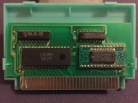
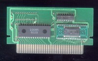
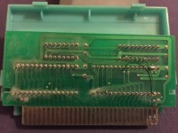
* This PCB was prepared for 32 pin EPROM (or mask ROM), additional wire and cut are for make 28 pin EPROM work.