Can you help getting more info about those carts?
| Unique visits: 7828 Can you help getting more info about those carts? |
|  |
| Name | Value |
|---|---|
| U1 | 27512 |
| U10 | AM29F040P |
| U11 | 74139 |
| U2 | AM29F040P |
| U3 | AM29F040P |
| U4 | AM29F040P |
| U5 | 6264 (not soldered)(6264) |
| U6 | 6264 |
| U7 | AX5202P(MMC3) |
| U8 | 74174 |
| U9 | 16L8 |
| C1 | 1n |
| CART1 | FAMICOM_CART |
| D1 | |
| JP1 | 1-2 |
| JP2 | 1-2 |
| JP3 | 1-2 |
| R1 | ? |


http://forums.nesdev.com/viewtopic.php?f=9&t=19390
[code]
Presumable order of ROM chunks:
PRG: 512 kB ROM (U2) + 512 kB ROM (U3) + 32 kB ROM (U1) + 8 kB RAM (U5, not soldered)
CHR: 512 kB ROM (U10) + 512 kB ROM (U4) + 8 kB RAM (U6)
[...A.BCD] $6000-$7fff - control register, set to 0 on powerup/reset
| |||
| ||+-- PRG/CHR-A17
| |+--- PRG/CHR-A18
| +---- PRG/CHR-A19
+------ ROM selection: 0=ROM with MENU U1, 1=ROMs with games (U2+U3)
+------ might also block further writes to this reg when set to 1 (needs pal analysis for confirmation)
PRG A16-A13: controlled by MMC3
PRG A17: controlled by PAL (can come from MMC3-PRG-A17 or from PAL)
PRG A18 = C
PRG A19 = B
CHR A16-A10: controlled by MMC3
CHR A17: controlled by PAL (can come from MMC3-PRG-A17 or from PAL)
CHR A18 = C
CHR A19 = B
Doubts:
* I don't see any bit determining if CHR-ROM or CHR-RAM should be applied.
Maybe it's hardcoded that for menu (REG=%00000) and for position 3 (REG=%10010)
it should enable RAM, otherwise ROM
* I don't see any bit determining if PRG A17/CHR A17 should come from MMC3 (bank size 256 kB)
or from PAL (bank size 128 kB)
* PAL's pin 18/19 are shorted
* Why does PAL need MMC3-PRG-!CE pin, if it already has wired CPU-!ROMSEL and CPU-R/!W?
PRG-ROM | PRG-RAM | CHR-ROM | CHR-RAM | $6000
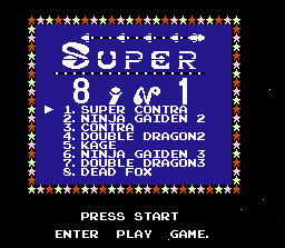
0. Menu | 32 kB | 0 | 0 | 8 kB | %00000 (relies on powerup value )
1. Super Contra | 128 kB | 0 | 128 kB | 0 | %10000
2. Ninja Gaiden 2 | 128 kB | 0 | 128 kB | 0 | %10001
3. Contra | 128 kB | 0 | 0 | 8 kB | %10010
4. Double Dragon 2 | 128 kB | 0 | 128 kB | 0 | %10011
5. Kage | 128 kB | 0 | 128 kB | 0 | %10100
6. Ninja Gaiden 3 | 128 kB | 0 | 128 kB | 0 | %10101
7. Double Dragon 3 | 128 kB | 0 | 128 kB | 0 | %10110
8. Dead Fox | 128 kB | 0 | 128 kB | 0 | %10111
.--v--. .-----------------------.
MMC3_PRG_nCE -> |01 20| -- VCC |01 +-1k------- 20|
M2 -> |02 19| -> CHR_RAM_CS |02 --<|--+ +----- 19|
CPU_nROMSEL -> |03 18| -> CHR_RAM_CS |03 --<|--+ +----- 18|
CPU_A14 -> |04 17| <- CPU_RnW |04 --<|--+ | 17|
CPU_A13 -> |05 16| -> CHR_A17 |05 --<|--+ | +- 16|
REG_D4 -> |06 15| -> CHR_RAM/nROM -> |06 -+-|) ------+----- 15|
REG_D2 -> |07 14| <- MMC3_CHR_A17 |07 +-|) | 14|
REG_D1 -> |08 13| -> PRG A17 |08 +- 13|
REG_D0 -> |09 12| -> REG_nWR |09 ---------------+ 12|
GND -- |10 11| <- MMC3_PRG_A17 |10 11|
'-----' '-----------------------'
PAL
Try replacing PAL with:
pin 9 -> short to both: pin 13, pin 16
pin 6 -> input1 of negattor
REG_nWR <= 0 when CPU_nROMSEL=1 and M2=1 and CPU_A14=1 and CPU_A13=1 and CPU_RnW=0 else 1
[/code]
If that's PAL failure, you can replace it with fresh new pre-programmed GAL.
But I'd check first U8.pin 1 voltage when cartridge is running (you don't have to solder all elements, just 74174, diode/resistor and capacitor).
[url=https://obrazki.elektroda.pl/1504938300_1571228073.png][img]https://obrazki.elektroda.pl/1504938300_1571228073_thumb.jpg[/img][/url] Comments: