Kyuukyoku Harikiri Stadium: Heisei Gannen Ban
Elements:
| Name | Value |
|---|
| IC1 | 27512 |
| IC2 | 27F080 |
| IC3 | X1-017 |
| BAT1 | CR2032 |
| C1 | 100n |
| C2 | 100n |
| C3 | 150p |
| CART1 | FAMICOM_CART |
| D1A | M21 |
| D1B | M21 |
| R1 | 330R |
| R2 | 1k |
| TP1 | |
| TP2 | |
| TP3 | |
| TP4 | |
Chip signature:
27512+27F080+X1-017
PCB top:
PCB bottom:

Shell top:
No photo
Shell bottom:
No photo
Screenshoots:
No photo
Extra info:
X1-017 testing
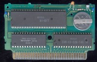
I got bought `[url=http://bootgod.dyndns.org:7777/profile.php?id=1767]Kyuukyoku Harikiri Stadium: Heisei Gannen Ban[/url]` game to test X1-017 chip. My IC is dated 8932KX.
[url=https://obrazki.elektroda.pl/7628879700_1580400210.jpg][img]https://obrazki.elektroda.pl/7628879700_1580400210_thumb.jpg[/img][/url] [url=https://obrazki.elektroda.pl/7255975400_1580400212.jpg][img]https://obrazki.elektroda.pl/7255975400_1580400212_thumb.jpg[/img][/url] [url=https://obrazki.elektroda.pl/3800109000_1580400247.png][img]https://obrazki.elektroda.pl/3800109000_1580400247_thumb.jpg[/img][/url]
I will post my observation results:
* Data pins seem to be internally pulled-down to GND by the X1-011 (much stronger than the internal 20k-50k pull-ups in atmega16 in kazzo), because reading from $0000-$5fff, $73400-$7fff returns 0x00. When particular RAM region is disabled, it also returns 0x00 in every byte from it.
* Stop of M2 toggling does not seem to disable any of RAM regions
* RAM EN/DIS registers aree fully decoded (there are no mirrors in $7800-$7fff)
* All NC pins are internally connected
* Looking at the following waveform we can conclude that PRG select registers ($7efa/7efb/7efc) are in fact 6 bit wide (bits 5..0 are utilized, not 7..2 as wiki says) and this mapper supports up to 512 kB of PRG-ROM:. THe order of bit is
pin62 -> $7efa.0 (PRG-A13)
pin60 -> $7efa.1 (PRG-A14)
pin61 -> $7efa.2 (PRG-A15)
pin59 -> $7efa.3 (PRG-A16)
pin58 -> $7efa.4 (PRG-A17)
pin1 -> $7efa.5 (PRG-A18)
[url=https://obrazki.elektroda.pl/7602003600_1580399978.png][img]https://obrazki.elektroda.pl/7602003600_1580399978_thumb.jpg[/img][/url]
* Pin 55 [strike](or 53)[/strike] - seem to be delayed M2 (both edges are delayed ~100ns)
* Pin 54 - seem to be delayed M2 (only rising edge is delayed ~100ns)
I think that pin 53 [strike](or 55)[/strike] is an input used for generating chip enable to the internal RAM. They were concerned about the M2/PRG_CE delay that might cause RAM corruption so they did the delaying circuit internally and drove it outside for manual selection which will work better. (I separated shorted pins 55+53 to find which one is input and which output)
[url=https://obrazki.elektroda.pl/7248307200_1580400036.png][img]https://obrazki.elektroda.pl/7248307200_1580400036_thumb.jpg[/img][/url]
[url=https://obrazki.elektroda.pl/7867324000_1580408159.png][img]https://obrazki.elektroda.pl/7867324000_1580408159_thumb.jpg[/img][/url] [url=https://obrazki.elektroda.pl/5714518000_1580408161.png][img]https://obrazki.elektroda.pl/5714518000_1580408161_thumb.jpg[/img][/url] [url=https://obrazki.elektroda.pl/6194274600_1580408163.png][img]https://obrazki.elektroda.pl/6194274600_1580408163_thumb.jpg[/img][/url]
Edit: Yes - after connecting pin 53 to GND, PRG/CHR register works normally, but RAM is always disabled. This confiirms that pin 53 is used only for decoding RAM,
--
Pin 34 is CHR_/CE (PPU_/RD or PPU_A13)
There is something weird with pins 56/46. WHen they're short, there is even more delayed (by half cycle) M2 on them:
[url=https://obrazki.elektroda.pl/2100347700_1580410628.png][img]https://obrazki.elektroda.pl/2100347700_1580410628_thumb.jpg[/img][/url]
But when I separate them, pin 46 is held HIGH and pin 56 is held LOW and mapper ignores writes to registers.
If the IRQ is functional, there is probably some latch value for the counter and this should be used as a reference for correct data bus bit order. I'll check that.
--
Pin45 = CHR_LO/CE (goes low when PPU_/RD=0 and PPU_A13=0 and CHR_A18 would be 0 for the actual CHR bank, else high
Pin44 = CHR_HI/CE (goes low when PPU_/RD=0 and PPU_A13=0 and CHR_A18 would be 1 for the actual CHR bank, else high
Those pins can be used if two DIL-28 128kB CHR-ROM chips with single /CE are used.
For example, if $7ef0 = $7ef2 = $7ef3 = $7ef4 = $7ef6 = $0, $7ef1 = $80 and we read the region $0000-$1fff, then we get:
[url=https://obrazki.elektroda.pl/9517792800_1580424290.png][img]https://obrazki.elektroda.pl/9517792800_1580424290_thumb.jpg[/img][/url]
--
7eff 73 1
7efe cf 1
7efe c8 1
7eff b7 1
7efe 59 1
7efe 5b 0
$7efd:
[VVVVVVV]
|||||||
+++++++-- reload value
7efe:
[.....?IE]
|||
||+- 1-enable counting, dont modify counter
|| 0-disable counting and set counter to ($7efd == 0) ? 17 : (($7efd + 2) * 16)
|+-- 1-enable IRQs, 0-disable IRQs
+-- this bit must be either also 0 to enable counting or it set clock source to
something other. however I wasn't able to make clocking work when it was
other than 1 (even if I toggled PPU_A12/PPU_/RD/PPU_A13)
7eff:
[........] - writing any value clears the IRQ pending flag and sets the counter to ($7efd == 0) ? 2 : ((($7efd + 1) * 16) + 1)
On every cpu cycle, if counting is enabled, counter is decreased. If it reaches 0, IRQ pending flag is set.
Can't tell if the counter wraps and still clocks, because acking IQR by writing to 7eff modifies counter value
IRQ is asserted asynchronicaly if both IRQ pending flag is set and I bit is set, for example:
$7efd <= 0x2
$7efe <= 0
$7eff <= 0
$7efe <= 1
now do at least 64 CPU clocks, /IRQ line will be still high after that. But writing $7efe <= 2 make it go instantly low.
Next write of 0 to $7efe will make /IRQ go high, but again write $7efe <= 2 will make it low, etc.
--
[quote=lidnariq post_id=246594 time=1580440980 user_id=3512]
Any chance pin 56 is actually an open-drain output? Maybe that's how they implemented reset detection? And the RC aren't just a cold reset detection, but the capacitor is periodically drained by pin 56 during operation, and if the resistor ever pulls the pin high, pin 46 disables RAM access?
[/quote]
You're genius. I should've cut it like on the left, not on the right.
[url=https://obrazki.elektroda.pl/2857305900_1580498770.png][img]https://obrazki.elektroda.pl/2857305900_1580498770_thumb.jpg[/img][/url]
Now (1=M2, 2=pin56+R+C) it indeed acts like a reset. But it rises up to 4V and it would trigger reset on every clock edge. pg[url=https://obrazki.elektroda.pl/8275360200_1580500129.png][img]https://obrazki.elektroda.pl/8275360200_1580500129_thumb.jpg[/img][/url]
Anyway, when I wre pin 46 to VCC, it still allows me to access RAM. I'm wondering if it's just write protection, not read protection.
-
I did more testing to the VBatteryBackup (pin 48), VBattery(pin 49) and Test Pad 2 (pin 50)
* Test Pad 2 is output pin: driven by 5V when the cartridge is powered from console (VbatteryBackup > Vbattery) is at 0v when the the cartridge is powered only by internal battery (VbatteryBackup < Vbattery). Probably it is a testing pad to check either if memory correctly switches to low-power mode or is it protected against writes when in battery backup mode.
* When the pin 49 is connected to the battery, chip sinks unmeasureable current rom battery through pin 48 (there is <0.01mV drop on serial 1k resistor meaning < 0.01mA)
* If pin 49 is disconnected from battery, pin 48 starts to sink 1.6mA from battery (maybe now chip thinks it is connected to non-battery supply)
-
Here is a comparision of M2(CH1), pin 56(CHR2), pin55 (CH3), pin54 (CHR4).
[url=https://obrazki.elektroda.pl/7227642200_1580639999.png][img]https://obrazki.elektroda.pl/7227642200_1580639999_thumb.jpg[/img][/url]
Pin 46 must be some kind of RAM+WE because when tied to GND, I wasnt able to modify any of RAM cells.
But there is something super crazy with the writing. I put the game in console and allow it to initialize the RAM. Then I put it into kazzo, wrote $ca to $6fe7 and read $6000-$67ff for the first time, second time and third time. 1st and 2nd reads differ, but 2nd and 3rd were the same. They differed on two positions - $6000 and $6400. It looked like value at $6000 is copy of what is at $63ff and at $6400 is copy of $67ff. I disconnected the Kazzo, connected it again and reads from $6000-$67ff were still the same as 2nd and 3rd.
I repeat the whole procedure again - put the cartridge in console, run game, then put it into kazzo and the result were the same as described above.
Moreover, In Kazzo I was not able to write anything at cells $6000 and $6400 - the value in them was always the copy of $63ff and $67ff. Plus the writes in Kazzo to RAM are very unreliable.
--
Also, the exact timing measurements:
pin 55 - Rising edge delayed of 71ns after rising of m2, falling edge delayed of 78ns
pin 54 - Rising edge delayed of 37ns after rising of m2, falling edge delayed of 40ns * = 1/0
7efd 00 | 7efd 00 | 7efd 00 | 7efd 00 | 7efd 00 | 7efd 00 | 7efd 00 | 7efd 00 | 7efd 00 | 7efd 00 | 7efd 00 | 7efd 00 |
7efe 00 | 7efe 00 | 7efe 00 | 7efe 00 | 7efe 00 | 7efe 00 | 7efe 00 | 7efe 00 | 7efe 00 | 7efe 00 | 7efe 00 | 7efe 00 |
7eff 00 | 7eff 00 | 7eff 00 | 7eff 00 | 7eff 00 | 7eff 00 | 7eff 00 | 7eff 00 | 7eff 00 | 7eff 00 | 7eff 00 | 7eff 00 |
7efd 01 | 7efd 00 | 7efd 00 | 7efd 00 | 7efd 00 | 7efd 00 | 7efd 00 | 7efd 00 | 7efd 00 | 7efd 00 | 7efd 00 | 7efd 00 |
7efe 00 | 7efe 00 | 7efe 00 | 7efe 00 | 7efe 00 | 7efe 00 | 7efe 00 | 7efe 00 | 7efe 00 | 7efe 00 | 7efe 00 | 7efe 00 |
7efe 03 | 7efe 03 | 7efe 03 | 7efe 03 | 7efe 03 | 7efe 03 | 7efe 03 | 7efe 03 | 7efe 03 | 7efe 03 | 7efe 03 | 7efe 03 |
48 | 17 | 7efd 00 | 7efd 01 | 7efd 01 | 7efd 01 | 7efe 03 | 7efe 01 | 7efe 00 | 7efe 04 | 7efe 05 | 7efe 03|
| | 16 | 47 | 7efd 01 | 7efd 01 | 7efe 03 | 7efe 03 | 7efe 03 | 7efe 03 | 7efe 03 | 7efe 03 |
| | | | 7efd 01 | 7efd 01 | 15 | 15 | 16 | 16 | 15 | 7eff 00 |
| 7efd 01 7efd 01 | 02
7efd 01 7efd 01 |
7efd 01 7efd 01 |
7efd 01 7efd 01 |
7efd 01 7efd 01 |
7efd 01 7efd 01 |
7efd 01 7efd 01 |
7efd 01 7efd 01 |
7efd 01 7efd 01 |
7efd 01 7efd 01 |
7efd 01 7efd 01 |
34 7efd 01 |
49 |
$7efd:
[VVVVVVV]
|||||||
+++++++-- set internal counter to written value + 1, do not modify prescaler
7efe:
[.....?IE]
|||
||+- 1-enable counting, 0-disable counting
++-- 01-enable IRQs, other-disable irqs
7eff:
[........] - writing any value clears the IRQ pending flag and sets prescaler to 0 Comments:
Want to leave a comment?