Can you help getting more info about those carts?
| Unique visits: 7975 Can you help getting more info about those carts? |
|  |
| Name | Value |
|---|---|
| IC1 | EF009-5B(27F080) |
| IC2 | EF009-5A(27F080) |
| IC3 | -(27F080) |
| IC4 | 6264 |
| IC5 | PST532A(DIL8) |
| BAT1 | CR2032 |
| C1 | - |
| C2 | - |
| C3 | 100n |
| C4 | 100n |
| CON1 | Konami-QTA |
| JPA | CLOSED |
| JPB | OPEN |
| JPC | OPEN |
| JPD | OPEN |
| JPE | CLOSED |
| JPF | CLOSED |
| JPH | CLOSED |
| JPI | OPEN |
| JPJ | OPEN |
| JPK | OPEN |
| JPL | CLOSED |
| JPM | CLOSED |
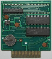
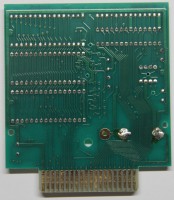
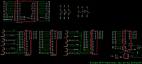
Sanchez sent me photos of both sides of the cartridge and adapter, so I was able to do my best and try to find-out the pinouts. I can't guarantee in 100% that all hidden connections were revealed correctly, but the VRC5 pin order seems to be quite logical (pins are in functional groups and in order)

Adapter:
[url=https://obrazki.elektroda.pl/7477397000_1567668293.jpg][img]https://obrazki.elektroda.pl/7477397000_1567668293_thumb.jpg[/img][/url] [url=https://obrazki.elektroda.pl/6283113400_1567668299.jpg][img]https://obrazki.elektroda.pl/6283113400_1567668299_thumb.jpg[/img][/url] [url=https://obrazki.elektroda.pl/9207505200_1567668302.jpg][img]https://obrazki.elektroda.pl/9207505200_1567668302_thumb.jpg[/img][/url] [url=https://obrazki.elektroda.pl/9473693500_1567668304.jpg][img]https://obrazki.elektroda.pl/9473693500_1567668304_thumb.jpg[/img][/url] [url=https://obrazki.elektroda.pl/4448299700_1567711081.png][img]https://obrazki.elektroda.pl/4448299700_1567711081_thumb.jpg[/img][/url]

Cartridge:
[url=https://obrazki.elektroda.pl/8876187700_1567668351.jpg][img]https://obrazki.elektroda.pl/8876187700_1567668351_thumb.jpg[/img][/url] [url=https://obrazki.elektroda.pl/8607980800_1567668354.jpg][img]https://obrazki.elektroda.pl/8607980800_1567668354_thumb.jpg[/img][/url] [url=https://obrazki.elektroda.pl/6974727700_1567668359.jpg][img]https://obrazki.elektroda.pl/6974727700_1567668359_thumb.jpg[/img][/url] [url=https://obrazki.elektroda.pl/3963487600_1567668361.jpg][img]https://obrazki.elektroda.pl/3963487600_1567668361_thumb.jpg[/img][/url] [url=https://obrazki.elektroda.pl/9905417500_1567668373.png][img]https://obrazki.elektroda.pl/9905417500_1567668373_thumb.jpg[/img][/url]

[code]
My notes/doubts:
* Both cartride and adapter contains a lot of jumpers, whose role is to
  switch between DIL32 / DIL28 ROMs
	Cartridge PCB (351384)
	--------------------------------------------------------------------
    IC2    JPC JPF JPB JPE JPD JPA
    DIL32  OPN CLS OPN CLS OPN CLS <- default (EF009-5A installed)
    DIL28  CLS OPN CLS OPN CLS OPN
    --------------------------------------------------------------------
    IC1                            <- always DIL32 (EF009-5B installed)
    --------------------------------------------------------------------
    IC3    JPJ JPM JPI JPL JPK JPH
    DIL32  OPN CLS OPN CLS OPN CLS <- default (non populated)
    DIL28  CLS OPN CLS OPN CLS OPN
	--------------------------------------------------------------------

	Adapter PCB (351383A)
	--------------------------------------------------------------------
	IC2    JPF JPG JPA JPC JPD JPE JPB JPH
	DIL28  OPN OPN OPN CLS CLS OPN CLS OPN <- default (EF901 installed)
	DIL32  CLS OPN CLS OPN CLS OPN OPN CLS
	--------------------------------------------------------------------
	IC3    JPN JPM JPL JPK
	DIL28  OPN CLS OPN CLS                 <- default (EF901-KN installed)
	DIL32  OPN CLS CLS OPN

* INT PRG ROM / INT PRG RAM refers to the internal chips
  (those inside adapter)

* EXT PRG ROM / EXT PRG RAM refers to the external chips
  (those inside cartridge that is plugged into adapter)

* Theoretically the maximum supported ROM sizes are:
   INT PRG ROM: 1 * 256 kiB
   EXT PRG ROM: 3 * 256 kiB
   INT CHR ROM: 128 kiB
   INT PRG RAM: 8 kiB
   EXT PRG RAM: 32 kiB ???

* Unknown pins:
    VRC5.68 = QTA.18 (might be PRG RAM A13)
	VRC5.80 = QTA.39 (might be PRG RAM A14)

* CHR-ROM chip (EF901-KN) has shuffled address lines and PPU A3 is not
  connected dirrectly but through VRC5 (is that something used to automatic
  japanese character switching?)

* What is Konami 052701 - regular 8k SRAM? Why they didnt use the same chip
  as for CHR-RAM or PRG-RAM? I analyzed other Konami Famicom PCBS and they
  never used RAM with Konami markings.

* There is one track on the adapter PCB that I don't have idea where goes to
 (and it seems to be surplus)
[/code]
[url=https://obrazki.elektroda.pl/7401728600_1567669267.jpg][img]https://obrazki.elektroda.pl/7401728600_1567669267_thumb.jpg[/img][/url]

[code]
                   Konami-QTA
                 Left=Label side
                    +-----+
             GND -- |01 21| -- VCC
          CPU A6 -> |02 22| <- CPU A8
         CPU A11 -> |03 23| <- CPU A9
          CPU A4 -> |04 24| <- CPU A5
          CPU A3 -> |05 25| <- CPU A10
          CPU A2 -> |06 26| <> CPU D7
         CPU A12 -> |07 27| <- CPU A7
          CPU D6 <> |08 28| <- CPU R/W
          CPU D5 <> |09 29| <- CPU A1
          CPU D4 <> |10 30| <- CPU A0
             GND -- |11 31| -- GND
          CPU D3 <> |12 32| <> CPU D0
          CPU D2 <> |13 33| <> CPU D1
         PRG A13 -> |14 34| <- PRG A14
         PRG A15 -> |15 35| <- PRG A16
EXT PRG ROM0 /CE -> |16 36| <- PRG A17
EXT PRG ROM1 /CE -> |17 37| <- EXT PRG ROM2 /CE
                  ? |18 38| <- PRG RAM A12
EXT PRG RAM /CE  -- |19 39| ?
             VCC -- |20 40| -- VCC
                    +-----+

                                  _____
                       CPU A8 -> /01 80\ ? (goes to QTA 39, maybe PRG RAM A14?)
                         VCC -- /02   79\ <> CPU D0
                     CPU A9 -> /03 (o) 78\ <> CPU D1
                   CPU A10 -> /04       77\ <> CPU D2
                  CPU A11 -> /05         76\ <> CPU D3
                 CPU A12 -> /06           75\ <> CPU D4
                CPU A13 -> /07             74\ <> CPU D5
               CPU A14 -> /08               73\ -- VCC
              CPU R/W -> /09                 72\ <> CPU D6
           CPU /RMSL -> /10                   71\ <> CPU D7
                 M2 -> /11                     70\ <- PPU /WE
               GND -- /12                       69\ <- PPU /RD
             /IRQ <- /13                         68\ ? (goes to QTA 18, maybe PRG RAM A13?)
         CIR A10 <- /14                           67\ -> PRG RAM A12
    CHR RAM A12 <- /15                             66\ -> EXT PRG ROM0 /CE
        PPU A3 -> /16                               65\ -> EXT PRG ROM1 /CE
       PPU D0 <> /17                                64/ -> EXT PRG ROM2 /CE
      PPU D1 <> /18                                63/ -- GND
     PPU D2 <> /19         VRC 5                  62/ -> INT PRG ROM /CE
    PPU D3 <> /20                                61/ -> PRG A17
   PPU D4 <> /21                                60/ -> PRG A16
  PPU D5 <> /22                                59/ -> PRG A15
    GND -- /23                                58/ -> PRG A14
PPU D6 <> /24                                57/ -> PRG A13
PPU D7 <> \25                               56/ -> QTRAM /WE
 PPU A7 -> \26                             55/ -> INT PRG RAM /CE
  PPU A8 -> \27                           54/ -> EXT PRG RAM /CE
   PPU A9 -> \28                         53/ -> CHR ROM A16
   PPU A10 -> \29                       52/ -- GND
    PPU A11 -> \30                     51/ -> CHR ROM A15
     PPU A12 -> \31                   50/ -> CHR ROM A14
      PPU A13 -> \32                 49/ -> CHR ROM A13
           VCC -- \33               48/ -> CHR ROM A12
      CIRAM /CE <- \34             47/ -> CHR ROM A11
       QTRAM +CE <- \35           46/ <> QTRAM D7
      CHR ROM /CS <- \36         45/ <> QTRAM D6
       CHR RAM /CS <- \37       44/ <> QTRAM D5
           QTRAM D0 <> \38     43/ <> QTRAM D4
            QTRAM D1 <> \39   42/ -- GND
             QTRAM D2 <> \40 41/ <> QTRAM D3
                          \   /
                           \ /
[/code]
Comments: