Sangokushi2 fs306
| Type | single | | Mapper | | | Original mapper | | | PCB marks | FS306 | | Tags: | | | Uploaded: | 2019-07-01 05:19:28 |
|  |
Elements:
Chip signature:
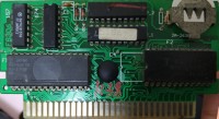
6264+6116L24+74157+74174+P_1(DIL20)+P_2(DIL20)+AX5208C(VRC4)+28F032+28F032
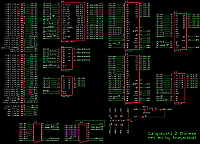
PCB top:

PCB bottom:


Shell top:
No photo
Shell bottom:
No photo
Screenshoots:
No photo
Extra info:
http://forums.nesdev.com/viewtopic.php?f=9&t=19041

I was thinking for a long time what chips they used for the PRG-ROM and CHR-ROM. Solving that could reveal how they routed the tracks underneath and which signals go to PALs. They definitely weren't blobs cause there weren't a empty (non-via) area in the center, so they must be TSOP chips.

My first candidate was 28f008 (found in [url=http://forums.nesdev.com/viewtopic.php?f=9&t=16124]ASDER PC-95 korean version[/url]).
[url=https://obrazki.elektroda.pl/5438257700_1562065321.jpg][img]https://obrazki.elektroda.pl/5438257700_1562065321_thumb.jpg[/img][/url]
But the pinout wasn't really fitting it well.
[img]https://obrazki.elektroda.pl/7504191600_1562064979.png[/img]

Neither the regular 29f040 did:
[img]https://obrazki.elektroda.pl/8100528800_1562064982.png[/img]

And then desperately looking at previous cartridges that I analyzed I found 28f032 (in `Fong Shen Bang - Zhu Lu Zhi Zhan (Mapper 246)` or `Genuine Monkey`)
[img]https://obrazki.elektroda.pl/8114241200_1562064978.png[/img]

This was a milestone, cause CHR-A18 was exactly needed in that place:
[img]https://obrazki.elektroda.pl/5049607000_1562065595.png[/img].

After that I was able to completely finish tracing the PCB and improve my previous ideas:
[url=https://obrazki.elektroda.pl/8669174600_1562065666.png][img]https://obrazki.elektroda.pl/8669174600_1562065666_thumb.jpg[/img][/url] [url=https://obrazki.elektroda.pl/3408714200_1562065670.png][img]https://obrazki.elektroda.pl/3408714200_1562065670_thumb.jpg[/img][/url] [url=https://obrazki.elektroda.pl/7595366300_1562065780.png][img]https://obrazki.elektroda.pl/7595366300_1562065780_thumb.jpg[/img][/url]

* VRC4 has its A13 and A14 connected directly to CPU-A13 and CPU-A14, making it behave normally
* 74174 latches D0..D5
* D0..D3 are connected to 74157 which multiplexes PRG-A13..A16 between those from VRC and 74174
* D4 is connected to P_1 which does the same
* D5 is not connected to anything
* VRC4 x=PPU_A13, y=PPU_!RD, z=CHR_!CE are used like OR gate (z = x || y).
* This OR gate is wired as following: x = CPU_A2, y = VRC-PIN18, z = 74174's clock, so that the 74174 sits at $9C00 (mask: $9C04)
* VRC4 does not control mirroring, this is the role of P_1. Its four disconnected pins would suggest that they contain latched D0 for the four nametables:
[code]
                P_1
             .---v---.
   CPU_A0 -> |01   20| -- VCC
   CPU_A1 -> |02   19| -> PRG_ROM_A17
   CPU_A2 -> |03   18| -> BANK_nREG/VRC
  CPU_A13 -> |04   17| <- REG_D4
  CPU_A14 -> |05   16|
VRC_PIN18 -> |06   15|
   CPU_D0 -> |07   14|
  PPU_A10 -> |08   13|
  PPU_A11 -> |09   12| -> CIRAM_A10
      GND -- |10   11| <- VRC_PRG_A17
             +-------+
[/code]

* Because $9c00.0 is already used for banking register, nametable regs sits at $9c04.0-$9c07.0 (mask: $9C04)

That would make the PAL equations like:
[code]
PIN13 <- CPU_D0 when VRC_PIN18 = 0 and CPU_A2 = 1 and CPU_A1 = 0 and CPU_A0 = 0 --latch

PIN14 <- CPU_D0 when VRC_PIN18 = 0 and CPU_A2 = 1 and CPU_A1 = 0 and CPU_A0 = 1 --latch

PIN15 <- CPU_D0 when VRC_PIN18 = 0 and CPU_A2 = 1 and CPU_A1 = 1 and CPU_A0 = 0 --latch

PIN16 <- CPU_D0 when VRC_PIN18 = 0 and CPU_A2 = 1 and CPU_A1 = 1 and CPU_A0 = 1 --latch

CIRAM_A10 <= PIN13 when PPU_A11 = 0 and PPU_A10 = 0 else
             PIN14 when PPU_A11 = 0 and PPU_A10 = 1 else
			 PIN15 when PPU_A11 = 1 and PPU_A10 = 0 else
			 PIN16

BANK_nREG/VRC <= 0 when CPU_A14 = 1 and CPU_A13 = 0 else 1
PRG_ROM_A17 <= REG_D4 when CPU_A14 = 1 and CPU_A13 = 0 else VRC_A17
[/code]

[code]
  +--------------------------------+
  |               P_2              |
  |            .---v---.           |
  +----------> |01   20| -- VCC    |
VRC_CHR_A11 -> |02   19| -> -------+
VRC_CHR_A12 -> |03   18| -> CHR-RAM-!CE
VRC_CHR_A13 -> |04   17| <- CHR-ROM-!CE
VRC_CHR_A14 -> |05   16|
VRC_CHR_A15 -> |06   15|
VRC_CHR_A16 -> |07   14|
VRC_CHR_A17 -> |08   13|
    PPU_!WE -> |09   12| <- PPU_A13
        GND -- |10   11| -- GND
               +-------+
[/code]

* Four not-connected pins (13-16) suggest that only four bits out of A17_A11 are latched (A10 and A18 is not taken into account at all)
* Probably PIN_19 <= 0 when PPU_A13 or PPU_!WE so that only writes to $0000-$1fff are treated as bank change


* I have no idea why P_2.pin11 is tied to GND

* the thick trace at P_1.pin17 suggested me that it was VCC signal, but I believe this was just a mistake with the thickness.
[url=https://obrazki.elektroda.pl/4974924100_1562067669.png][img]https://obrazki.elektroda.pl/4974924100_1562067669_thumb.jpg[/img][/url]
Comments:
Want to leave a comment?