Shell bottom: No photoScreenshoots: No photoExtra info:
https://www.nesdev.org/wiki/INES_Mapper_012
Just saw [url=https://www.nesdev.org/wiki/INES_Mapper_012]wiki article[/url] about this mapper.
Huang-1 has identical pinout to the [url=https://www.nesdev.org/wiki/C5052-13_pinout]C5052-13[/url].
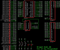
GAL16V8 is connected as follows:
[code]
+-------------------------------------------+
| +---v---+ |
+->- CLK_IN -> |01 20| -- VCC |
CPU_D1 -> |02 19| -> CLK_OUT ->------+
CPU_nROMSEL -> |03 18| -> CHR_A18
CPU_A14 -> |04 17| -> MPR_PPU_A12
CPU_A13 -> |05 16| -> MPR_MODE
CPU_A8 -> |06 15| -> O2 (feedb)
CPU_RnW -> |07 14| -> O3 (feedb)
PPU_A12 -> |08 13| <- CPU_D4
M2 -> |09 12| <- CPU_D0
GND -- |10 11| <- GND (/nOE)
+-------+
GAL16V8
CLK_OUT <= '0' when CPU_M2 = '1' AND CPU_NROMSEL = '1' AND CPU_A14 = '1' AND CPU_A13 = '1' AND CPU_A8 = '1' AND CPU_RNW = '0' ELSE '1';
O2.D := CPU_D0
O2.CLK := CLK_IN
O3.D := CPU_D4
O3.CLK := CLK_IN
MPR_MODE.D := CPU_D1
MPR_MODE.CLK := CLK_IN
CHR_A18 <= O2.D WHEN PPU_A12 = '0' ELSE O3.DS
[/code]
There can't be any solder jumper underneath PAL for language select, because all PAL pins are already used
But this GAL also controls Huang's MODE pin (VCC=MMC3, GND=VRC2, NC=MMC1) and it has CPU D1 routed in, which wiki does not mention.
Because this game always writes to $4132 with bit 1 set, I assume that state of this bit is direcftly latched to the MPR_MODE pin.
[code]
D~7654 3210 (write)
---------
...B ..MA
| |+- CHR A18 when PPU A12=0
| +-- MODE: MMC3=1, others = ??? (can be low or highimpedance)
+------ CHR A18 when PPU A12=1
[/code]
Whichi is also unclear for me, why this PAL constrols HUANG's PPU-A12.