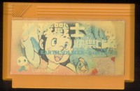
Happy Bichi
| Type | single | | Mapper | 4 | | Original mapper | | | PCB marks | 43-308 850646C T9553 | | Tags: | | | Uploaded: | 2023-02-04 04:31:15 |
|  |
Elements:
Chip signature:
27F080+27F080+6264+AX5202P(MMC3)+T9553(DIL32)
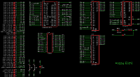
PCB top:
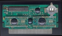

PCB bottom:

Shell top:
Shell bottom:

Screenshoots:
Extra info:
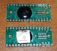
There are two "epoxy blob 32 pin" CHR memories, soldered one on top of the other. At first I thought, they are 128 kB each making total of 256 kB, but after desoldering and closer examination I found that bottom memory has only D4..D7 pins connected and top one - only D0..D3 (other data pins are milled out so they don't make connection).
I was wondering what is stored in those "not connected" data pins, so desoldered each of them and then read them back
chr-bottom [d4-d7 wired].BIN
chr-top [d0-d3 wired].bin

As you can see in comparision, "chr-bottom [d4-d7 wired]" has some internal breakup - in every 256 byte block, first 16 bytes has D2..D0 always set high.
I don't think this is some kind of "fix". Rather intentional behaviour (you need to have both roms soldered in order for game to be OK)

chr.bin is the merge of those bin's in a way it reflects their physical connection)

Next interesting thing is the T9553 epoxy blob - it inputs MMC3-CHR A17..A12 and MMC3-PRG A17..A14 (as well as CPU D2..D0, R/W, ROMSEL, M2, CPU A14..A12) and drives PRG A17..A14 and CHR A17..A12.

I don't know yet if this is a permanent behaviour or can be configured, but after power up, it shuffles MMC3 bits controlling PRG and CHR banks:
[code]
76543210 <- $8001 for PRG banks
|||||||+- PRG A13 (always)
||||||+-- PRG A17
   ||+--- PRG A14
   |+---- PRG A16
   +----- PRG A15

76543210 <- $8001 for CHR banks
|||||||+- CHR A10 (always)
||||||+-- CHR A11 (always)
|||||+--- CHR A13
||||+---- CHR A14
|||+----- CHR A15
||+------ CHR A17
|+------- CHR A12
+-------- CHR A16
[/code]

Happy Bichi [roms read from programmer].nes is pure merge of prg.bin + chr.bin
Happy Bichi [prg+chr bits reordered].nes is after applying those shuffling.
Comments:
Want to leave a comment?