Fuzhou Coolboy
| Type | single | | Mapper | | | Original mapper | | | PCB marks | FS006V3 | | Tags: | | | Uploaded: | 2023-02-04 09:29:18 |
| 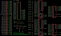 |
Elements:
| Name | Value |
|---|
| IC1 | 62256 |
| IC2 | 62256 |
| IC3 | 29LV160/320/640 |
| IC4 | 29LV160/320/640 |
| IC5 | DIL64 |
| BAT1 | CR2032 |
| C1 | ? |
| CART1 | FAMICOM_CART |
| D1 | |
| D2 | |
| D3 | - |
| D4 | - |
| JP1 | CLS |
| R1 | 2.2k |
| R2 | 10k |
| TP1 | TP |
| TP10 | TP |
| TP11 | TP |
| TP12 | TP |
| TP13 | |
| TP14 | |
| TP15 | TP |
| TP16 | TP |
| TP17 | TP |
| TP18 | TP |
| TP19 | TP |
| TP2 | TP |
| TP3 | TP |
| TP4 | TP |
| TP5 | TP |
| TP6 | TP |
| TP7 | TP |
| TP8 | TP |
| TP9 | TP |
Chip signature:
62256+62256+29LV160/320/640+29LV160/320/640+DIL64
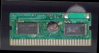
PCB top:
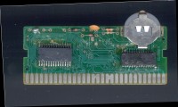
PCB bottom:
Shell top:
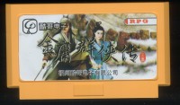
Shell bottom:
Screenshoots:
Extra info:
There was some horrible soldering of the chips, after applying fresh tin, it started to work.
The PCB is capable of supporting up to 1MB PRG and 512 kB CHR,
though only 512 kB PRG and 256 kB CHR are soldered.
It's basically MMC3 with some enhancement. When it detects no activity on M2 line,
it resets all its registers back to 0 (just as upon powerup).

From CPU BUS, it inputs CPU A14..12 and A4..A0.

From what I observed, there are at least those registers:

 76543210  PRG/CHR mode
[.tuv.qrs] @ $5010/$5014/$5018/$501c / mask: $F013 / power-on & reset: $00
  ||| +++---- PRG mode
  +++-------- CHR mode

 76543210  PRG bank
[..ABCDEF] @ $5011/$5015/$5019/$501d / mask: $F013 / power-on & reset: $00
   ++++++---- outer PRG bits

 76543210  CHR bank
[..QPRSTU] @ $5012/$5016/$501a/$501e / mask: $F013 / power-on & reset: $00
   ++++++---- outer CHR bits

 76543210  Enhanced MMC3 mode
[........] @ $5013/$5017/$501b/$501f / mask: $F013
 ++++++++---- additional banks for MMC3 mode: 0x02 = yes, others = no (all 8 bits matter)
              when "yes", $8000 can be also $8,$9,$a,$b

 76543210  Bank register select
[--..----] @ $8000 / mask: $E003 / power-on & reset: $00
 ++--|+++- when MMC3 enhanced mode is off
 ++--++++- when MMC3 enhanced mode is on

 76543210  Bank register value
[--------] @ $8001 / mask: $E003 / power-on & reset: $00 for all internal 12 regs
 ++++++++-  there are 12 internal registers that can be accessed by writing here

 76543210  UNROM latch / power-on & reset: $00
[.....yyy] @ $8000-$ffff / mask: $8000

 76543210  Mirroring
[......mm] @ $A000 / mask: $E003 / power-on & reset: $00
       ++---- mirroring (00=V, 01=H, 10=1scA, 11=1scB

 76543210  WRAM config
[abcdefgh] @ $A001 / mask: $E003 / power-on & reset: %01????0??
 |||  ||+--- PRG RAM A13
 |||  |+---- PRG RAM A14
 |||  +----- CHR memory type (0=ROM, 1=8kB RAM; both memories are banked in identical way)
 |++-------- WRAM banking mode
 |+--------- whats at $5xxx: 0=WRAM & writes to $5xxx regs blocked, 1=regs & writes to them allowed
 +---------- WRAM enabled (0=no, 1=yes)

         WRAM memory map
   | $5000-$5fff | $6000-$7fff
bc |   A14 A13   |   A14 A13
00 |    0   0    |    0   1
01 |    h   0    |    h   1
10 |  open bus   |    0   0
11 |  open bus   |    g   h
                      |   +---- = (c & h) | (!b)
                      +-------- = (b & c & g) | (!b & c & h)
Notes:
* Because RAM A12 is wired to CPU A12, $5000-$5fff maps always to second half of the 8kB bank seected by A14/A13
* 62256 pin 26 = A13, 6264 pin 26 = +CE so depending which chip is soldered in the cartridge, it
  can affect the behaviour:
    - 62256: values of $80/$c0 switch between two different banks at $6000-$7fff,
    - 6264: only $80 allows access to RAM (for $c0, it is disabled)
* there is no WRAM write protection bit in original MMC3 (though for some reason,
  WRAM /WE is driven by mapper, not by CPU R/W)

PRG MAP (fedcba = bits coming from MMC3: f = A18, ..., a = A13)
qrs |  $8000   $a000   $c000   $e000
000 | Afedcba Afedcba Afedcba Afedcba (512kB MMC3 PRG)
001 | ABedcba ABedcba ABedcba ABedcba (256kB MMC3 PRG)
010 | ABCdcba ABCdcba ABCdcba ABCdcba (128kB MMC3 PRG)
011 | ABCDEF0 ABCDEF1 ABCDEF0 ABCDEF1 (16kB NROM)
100 | ABCDE00 ABCDE01 ABCDE10 ABCDE11 (32kB NROM)
101 | ABCyyy0 ABCyyy1 ABC1110 ABC1111 UNROM
110 | 0000000 0000000 0000000 0000000
111 | 0000000 0000000 0000000 0000000

Notes:
- Writes to UNROM reg take effect even if not in UNROM mode as well as writes to
  all MMC3 regs take effect even not in MMC3 mode


CHR MAP (hgfedcba = bits coming from MMC3: h = A17, ..., a = A10)
tuv  | $0000/$0400/$0800/$0c00/$1000/$1400/$1800/$1c00
000  | Qhgfedcba (256kB MMC3 CHR)
001  | QPgfedcba (128kB MMC3 CHR)
010  | QPgfedcba (128kB MMC3 CHR)
011  | QPRSTU### (one 8kB bank)
1**  | QPRSTU### (one 8kB bank)

CHR can be RAM on ROM depending on A001.2.
IF PRG mode is 101, CHR is always RAM

(this need to be verified)

On my console, the cartridge has garbled graphics, probably because PPU /RD is not
wired to anything so I should add that fix in order to make it work on chipped consoles:

                 VCC
                  |
                 4.7k
                  |                 PPU A13 | PPU /RD | PPU /WR | CART PPU A13
PPU A13 -|>-------+--CART PPU A13       1   |    x    |    x    |      1
                  |                     0   |    0    |    x    |      0
PPU /RD -<|--470R-+                     0   |    x    |    0    |      0
PPU /WR -<|--470R-+                     0   |    1    |    1    |      1


--

Game on powerup does those writes:
$a001 $a1
$5000 $12
$5010 $8c
$5013 $f9

and later somewhere in code
$a001 $ec
$a001 $ed
$a001 $ee


Differences on what wiki says:
* a001.6 must be 1 on powerup/reset, because writes to $5xxx regs are enabled
* setting PRG mode to 101 forces CHR to be RAM, ignoring $a001.2
* all of those regs are zero on power-up & reset:
$8001.R0, $8001.R1, $8000.R2, $8000.R3, $8000.R4, $8000.R5, $8000.R6, $8000.R7, $8000.R8, $8000.R9, $8000.Ra, $8000.Rb
* miroring always can be selected between V/H/0/1, no matter of $a001

My notes:
* mapper inputs A2-A3 are ignored (every register is mirrored across them)
Comments:
Want to leave a comment?