Can you help getting more info about those carts?
| Unique visits: 7882 Can you help getting more info about those carts? |
|  |
| Name | Value |
|---|---|
| U1 | AX5208C(VRC4) |
| U2 | 16V8 |
| U3 | 27F080 |
| U4 | 27F080 |
| C1 | ? |
| C2 | - |
| C3 | - |
| C4 | - |
| C5 | - |
| C6 | - |
| C7 | - |
| CART1 | FAMICOM_CART |
| R1 | 510R |
| R2 | 1k |
| R3 | 2k |
| R4 | 3,9k |
| R5 | 1k |
| R6 | 10k |


The whole story started when trying to make repro of City Fighter 4 ([url=http://wiki.nesdev.com/w/index.php/NES_2.0_Mapper_266]mapper 266[/url])
[img]https://obrazki.elektroda.pl/2514959500_1608423589.png[/img] [img]https://obrazki.elektroda.pl/8600890500_1608423591.png[/img]
Thanks to wiki, I was able to get how the registers works. It does not say however how the DAC is realized so I made a resistor ladder:
[url=https://obrazki.elektroda.pl/2766966600_1608423764.jpg][img]https://obrazki.elektroda.pl/2766966600_1608423764_thumb.jpg[/img][/url] [url=https://obrazki.elektroda.pl/4179655900_1608423765.png][img]https://obrazki.elektroda.pl/4179655900_1608423765_thumb.jpg[/img][/url] [url=https://obrazki.elektroda.pl/1037734100_1608423771.png][img]https://obrazki.elektroda.pl/1037734100_1608423771_thumb.jpg[/img][/url]
https://www.youtube.com/watch?v=Dcj0r5pjIVc
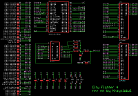
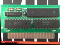
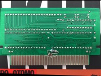
Then, somebody shown me how the original PCB looks like so I made a schematic:
[url=https://obrazki.elektroda.pl/4363537200_1608423852_org.jpg][img]https://obrazki.elektroda.pl/4363537200_1608423852_thumb.jpg[/img][/url] [url=https://obrazki.elektroda.pl/5192091600_1608423854_org.jpg][img]https://obrazki.elektroda.pl/5192091600_1608423854_thumb.jpg[/img][/url] [url=https://obrazki.elektroda.pl/1460149800_1608423862_org.jpg][img]https://obrazki.elektroda.pl/1460149800_1608423862_thumb.jpg[/img][/url] [url=https://obrazki.elektroda.pl/5117277600_1608423880.png][img]https://obrazki.elektroda.pl/5117277600_1608423880_thumb.jpg[/img][/url] [url=https://obrazki.elektroda.pl/2854090000_1608424999_org.jpg][img]https://obrazki.elektroda.pl/2854090000_1608424999_thumb.jpg[/img][/url]
There are some interesting facts:
* PRG ROM D3 and D5 are reversed (copy protection?)
* The resistor ladder is different than mine.
* Wiki says about using pin /WR900C of VRC4 to decode $900C/$980C, which sounds logical, because together with VRC4's OR gate and CPU-A11 it would work indeed:
[code]
CPU-A11 - |VRC4 OR A VRC4 OR Y | - WR9800C
+- |VRC4 OR B |
| | |
| | /WR900C| -+
| |
+------------------------------+
[/code]
but instead, PAL is used to perform the decoding and latch six bits (four for AUDIO DAC and two for PRG data)
* Despite using 32kB PRG banks (which would suggest that VRC4 is not involved in PRG banking at all), VRC4 drives PRG-A13 and PRG-A14. To make 32KB banks works as expected:
[code]
$8000 $a000 $c000 $e000
0 1 2 3
[/code]
game should initialize:
* PRG REG0 at $8000 to 0
* PRG REG1 at $a000 to 1 (which is accessed at $c000 because of mixed CPU-A13 and CPU-A14)
and it does it!
[code]
01:FE96: A9 00 LDA #$00
01:FE98: 8D 98 93 STA $9398
01:FE9B: 8D A0 86 STA $86A0 !
...
01:FE9E: A9 01 LDA #$01
01:FEA0: 8D 30 CD STA $CD30 !
[/code]
NewRisingSun - you made the wiki description of Mapper 266. Do you have different revision of this cartridge?Comments: