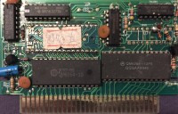
CSM04048N Speech chip (Sunsonic Educational Computer Learning Card)
| Type | single | | Mapper | 241 | | Original mapper | 241 | | PCB marks | | | Tags: | #audio | | Uploaded: | 2020-02-28 11:32:57 |
|  |
Elements:
| Name | Value |
|---|
| IC1 | 6264 |
| IC2 | 6264 |
| IC3 | 27F080 |
| IC4 | 7420 |
| IC5 | 74273 |
| IC6 | CSM04048N(DIL16) |
| IC7 | 7404 |
| IC8 | 16V8 |
| C1 | 2.2u |
| C2 | 100n |
| C3 | ? |
| C4 | - |
| CART1 | FAMICOM_CART |
| D1 | hack |
| D2 | hack |
| D3 | |
| D4 | |
| D5 | |
| JP1 | hack |
| JP2 | hack |
| JP3 | hack |
| JP4 | CLOSED |
| R1 | 1k (hack) |
| R10 | ? |
| R2 | 100k |
| R3 | 47k |
| R4 | 47k |
| R5 | 1k |
| R6 | 10k |
| R7 | 10k |
| R8 | 100k (-) |
| R9 | - |
| T1 | C945 |
| T2 | C9012 |
| T3 | - |
Chip signature:
6264+6264+27F080+7420+74273+CSM04048N(DIL16)+7404+16V8
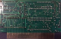
PCB top:

PCB bottom:
Shell top:
No photo
Shell bottom:
No photo
Screenshoots:

Extra info:
http://forums.nesdev.com/viewtopic.php?f=9&t=19793&p=247330#p247330

I tried to trace the board - schematics (that might need corrections):
[url=https://obrazki.elektroda.pl/9685832300_1582984261.png][img]https://obrazki.elektroda.pl/9685832300_1582984261_thumb.jpg[/img][/url]

[code]
$5000-$5fff: communication (read/write) with audoi chip

$6000-$7fff: RAM

$8000-$ffff (no bus conflicts):
[M...PPPP]
 |   ||||
 |   ++++- 32kB PRG bank at $8000-$ffff
 +-------- goes to mising PAL (mirroring control?)

          .---v---.
CPU D3 <> |01   16| <> CPU D7
CPU D2 <> |02   15| -- GND
CPU D1 <> |03   14| <> CPU D4
CPU D0 <> |04   13| ?? NC
   GND -- |05   12| -> AUDIO2 (not used)
CPU D6 -> |06   11| -> AUDIO1
    NC ?? |07   10| -- +5V
   /CE -> |08   09| <- R/w
          '-------'
[/code]

It perfectly matches the blob audio chip from [url=https://forums.nesdev.com/viewtopic.php?f=9&t=18248]subor sb-97 computer[/url], except that some data pins are shuffled, not all are used ant second audio channel is not wired.

I'm also quite interested with the mising PAL. Except that it could generate enable signal to the register at $8000, it can control CHR-RAM-A3 (?) and CHR-RAM-A12, which are not directly wired to PPU address lines. PAL watches PPU-A9, PPU-A3 (?), PPU-A0 (?). Would that mind to be used to make automatic CHR-RAM bank switch in middle of screen, just like [url=http://wiki.nesdev.com/w/index.php/Talk:INES_Mapper_163] Mapper 163 does?[/url]

MLX, can you confirm the connections 1-2-3-4 and  tell where the line 5 goes behind the capacitor?
[url=https://obrazki.elektroda.pl/8700168500_1582985204.jpg][img]https://obrazki.elektroda.pl/8700168500_1582985204_thumb.jpg[/img][/url]
Comments:
Want to leave a comment?