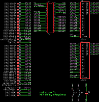
logoUnique visits: 7962
Can you help getting more info about those carts?
Cart name
Notes for chip search:
  • Use "+" as delimeter for all fields (except "cart name", where space is used); if many values are entered, all of them must appear in the cartridge then; case is not sensitive
  • "Mapper" is the actual mapper used by this cartridge hardware (might not match the one at wiki.nesdev.com, as at the moment I was analyzing this cartridge, there was no mapper assigned to it, so I had to assign my own number for testing)
  • "Original mapper" is the mapper used by licensed version of this game (for multicarts, it refers to mapper of the inside games, so 0+2 means this cartridge can run NROM+UNROM games)
  • Order in which you put values doesn't matter (you can write 7400+74138+7400 or 7400+7400+74138 to search for a cartridge that contains at least two 7400 chips and one 74138
  • Some chips (like PAL16*8) appear in cartridges as 16V8 or 16L8, so be sure to check both posibilities
  • Same goes for memories - type 27F080 to search for 32 pin memories, 27512 for 28 pin with two chip enables or MASKROM_1M_DIP28 for 28 pin with one chip enable
  • Same goes for mappers - some examples: AX5904(MMC1), AX5202P(MMC3), PT8154BM (9112MMC3), AX5208C(VRC4), 23C3662(VRC2)
  • Good news is that you can use wildcards, so 74139+*MMC3* will search for any cartrige that has at least one 74139 and MMC3 chip in any version
Mapper#
Original mapper#
PCB marks
Tags
Chips
Terminator 2 - Judgement Day
Typesingle
Mapper4
Original mapper4
PCB marksFC-26 5050
Tags:
Uploaded:2021-01-25 04:35:33

Elements:
NameValue
IC127F080
IC227F080
IC3T1(DIL40)
C1-
CART1FAMICOM_CART

Chip signature:
27F080+27F080+T1(DIL40)

PCB top:

PCB bottom:

Shell top:
No photo

Shell bottom:
No photo
Screenshoots:

Extra info:
             .--\/--.              
       M2 -> |01  40| -- VCC   
  CPU R/W -> |02  39| <- PPU A10
  /ROMSEL -> |03  38| <- PPU A11
 WRAM +CE <- |04  37| <- PPU A12  
 WRAM /CE <- |05  36| <- CPU A0  
 WRAM /WE <- |06  35| <- CPU A13   
  PRG /CE <- |07  34| <- CPU A14   
   CPU D0 -> |08  33| -> /IRQ   
   CPU D1 -> |09  32| -> DELAYED M2
   CPU D2 -> |10  31| -> CIR A10   
   CPU D3 -> |11  30| -> CHR A17   
   CPU D4 -> |12  29| -> CHR A15   
   CPU D5 -> |13  28| -> CHR A14  
   CPU D6 -> |14  27| -> CHR A13  
   CPU D7 -> |15  26| -> CHR A12
  PRG A13 <- |16  25| -> CHR A11  
  PRG A14 <- |17  24| -> CHR A10   
  PRG A15 <- |18  23| -> CHR A16  
  PRG A16 <- |19  22| -> PRG A18   
      GND -- |20  21| -> PRG A17   
             '------'              
                T1
			   
* Pins 4 and 5 are normally disabled (pin4 = 0, pin5 = 1). They are asserted (pin4 = 1, pin5 = 0):
- during read cycle from $6000-$7fff when $A001.7=1
- during write cycle to $6000-$7fff when $A001.7=1 and $A001.6=0
* Pins 4 and 5 are asserted 110ns after M2 goes up and deasserted 20ns after M2 goes down
* Pin 6 is asserted around 180ns after M2 goes up and  deasserted 20ns after M2 goes down
* There does not seem to be any consistent power-up value for the $a001
* Pin 6 is low when when R/W=0 and M2=1, no matter what $A001 is
* Pin 32 goes up 100ns after M2 goes up and goes down 80ns after M2 goes down

Comments:

Want to leave a comment?

Name:

Page loaded in 0.8 seconds | W3C validate